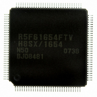
DF61654N50FTV Renesas Electronics America, DF61654N50FTV Datasheet - Page 243

DF61654N50FTV
Manufacturer Part Number
DF61654N50FTV
Description
IC H8SX/1654 MCU FLASH 120TQFP
Manufacturer
Renesas Electronics America
Series
H8® H8SX/1600r
Datasheet
1.DF61653N50FTV.pdf
(1020 pages)
Specifications of DF61654N50FTV
Core Processor
H8SX
Core Size
32-Bit
Speed
50MHz
Connectivity
I²C, IrDA, SCI, SmartCard, USB
Peripherals
DMA, PWM, WDT
Number Of I /o
75
Program Memory Size
512KB (512K x 8)
Program Memory Type
FLASH
Ram Size
40K x 8
Voltage - Supply (vcc/vdd)
3 V ~ 3.6 V
Data Converters
A/D 8x10b; D/A 2x8b
Oscillator Type
External
Operating Temperature
-20°C ~ 75°C
Package / Case
120-TQFP, 120-VQFP
For Use With
HS0005KCU11H - EMULATOR E10A-USB H8S(X),SH2(A)3DK1657 - DEV EVAL KIT FOR H8SX/1657
Lead Free Status / RoHS Status
Lead free / RoHS Compliant
Eeprom Size
-
Available stocks
Company
Part Number
Manufacturer
Quantity
Price
Company:
Part Number:
DF61654N50FTV
Manufacturer:
Renesas Electronics America
Quantity:
10 000
- Current page: 243 of 1020
- Download datasheet (6Mb)
6.8
In this LSI, external address space areas 0 and 1 can be designated as burst ROM space, and burst
ROM interfacing performed. The burst ROM interface enables ROM with page access capability
to be accessed at high speed.
Areas 1 and 0 can be designated as burst ROM space by means of bits BSRM1 and BSRM0 in
BROMCR. Consecutive burst accesses of up to 32 words can be performed, according to the
setting of bits BSWDn1 and BSWDn0 (n = 0, 1) in BROMCR. From one to eight cycles can be
selected for burst access.
Settings can be made independently for area 0 and area 1.
In the burst ROM interface, the burst access covers only CPU read accesses. Other accesses are
performed with the similar method to the basic bus interface.
6.8.1
Burst ROM interface can be specified for areas 0 and 1. Areas 0 and 1 can be specified as burst
ROM space by setting bits BSRMn (n = 0, 1) in BROMCR.
6.8.2
The bus width of the burst ROM space can be specified as 8-bit or 16-bit burst ROM interface
space according to the ABWHn and ABWLn bits (n = 0, 1) in ABWCR.
For the 8-bit bus width, data bus (D7 to D0) is valid. For the 16-bit bus width, data bus (D15 to
D0) is valid.
Access size and data alignment are the same as the basic bus interface. For details, see section
6.5.6, Endian and Data Alignment.
Burst ROM Interface
Burst ROM Space Setting
Data Bus
Rev.1.00 Sep. 08, 2005 Page 193 of 966
Section 6 Bus Controller (BSC)
REJ09B0219-0100
Related parts for DF61654N50FTV
Image
Part Number
Description
Manufacturer
Datasheet
Request
R

Part Number:
Description:
KIT STARTER FOR M16C/29
Manufacturer:
Renesas Electronics America
Datasheet:

Part Number:
Description:
KIT STARTER FOR R8C/2D
Manufacturer:
Renesas Electronics America
Datasheet:

Part Number:
Description:
R0K33062P STARTER KIT
Manufacturer:
Renesas Electronics America
Datasheet:

Part Number:
Description:
KIT STARTER FOR R8C/23 E8A
Manufacturer:
Renesas Electronics America
Datasheet:

Part Number:
Description:
KIT STARTER FOR R8C/25
Manufacturer:
Renesas Electronics America
Datasheet:

Part Number:
Description:
KIT STARTER H8S2456 SHARPE DSPLY
Manufacturer:
Renesas Electronics America
Datasheet:

Part Number:
Description:
KIT STARTER FOR R8C38C
Manufacturer:
Renesas Electronics America
Datasheet:

Part Number:
Description:
KIT STARTER FOR R8C35C
Manufacturer:
Renesas Electronics America
Datasheet:

Part Number:
Description:
KIT STARTER FOR R8CL3AC+LCD APPS
Manufacturer:
Renesas Electronics America
Datasheet:

Part Number:
Description:
KIT STARTER FOR RX610
Manufacturer:
Renesas Electronics America
Datasheet:

Part Number:
Description:
KIT STARTER FOR R32C/118
Manufacturer:
Renesas Electronics America
Datasheet:

Part Number:
Description:
KIT DEV RSK-R8C/26-29
Manufacturer:
Renesas Electronics America
Datasheet:

Part Number:
Description:
KIT STARTER FOR SH7124
Manufacturer:
Renesas Electronics America
Datasheet:

Part Number:
Description:
KIT STARTER FOR H8SX/1622
Manufacturer:
Renesas Electronics America
Datasheet:

Part Number:
Description:
KIT DEV FOR SH7203
Manufacturer:
Renesas Electronics America
Datasheet:


