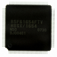
DF61654N50FTV Renesas Electronics America, DF61654N50FTV Datasheet - Page 852

DF61654N50FTV
Manufacturer Part Number
DF61654N50FTV
Description
IC H8SX/1654 MCU FLASH 120TQFP
Manufacturer
Renesas Electronics America
Series
H8® H8SX/1600r
Datasheet
1.DF61653N50FTV.pdf
(1020 pages)
Specifications of DF61654N50FTV
Core Processor
H8SX
Core Size
32-Bit
Speed
50MHz
Connectivity
I²C, IrDA, SCI, SmartCard, USB
Peripherals
DMA, PWM, WDT
Number Of I /o
75
Program Memory Size
512KB (512K x 8)
Program Memory Type
FLASH
Ram Size
40K x 8
Voltage - Supply (vcc/vdd)
3 V ~ 3.6 V
Data Converters
A/D 8x10b; D/A 2x8b
Oscillator Type
External
Operating Temperature
-20°C ~ 75°C
Package / Case
120-TQFP, 120-VQFP
For Use With
HS0005KCU11H - EMULATOR E10A-USB H8S(X),SH2(A)3DK1657 - DEV EVAL KIT FOR H8SX/1657
Lead Free Status / RoHS Status
Lead free / RoHS Compliant
Eeprom Size
-
Available stocks
Company
Part Number
Manufacturer
Quantity
Price
Company:
Part Number:
DF61654N50FTV
Manufacturer:
Renesas Electronics America
Quantity:
10 000
- Current page: 852 of 1020
- Download datasheet (6Mb)
Section 20 Flash Memory (0.18-µm F-ZTAT Version)
7. Initialization is executed. The initialization program is downloaded together with the
8. The return value in the initialization program, the FPFR parameter is determined.
9. All interrupts and the use of a bus master other than the CPU are disabled during
10. FKEY must be set to H'5A and the user MAT must be prepared for programming.
Rev.1.00 Sep. 08, 2005 Page 802 of 966
REJ09B0219-0100
programming program to the on-chip RAM. The entry point of the initialization program is at
the address which is 32 bytes after #DLTOP (start address of the download destination
specified by FTDAR). Call the subroutine to execute initialization by using the following
steps.
MOV.L #DLTOP+32,ER2
JSR
NOP
The general registers other than ER0 or ER1 are held in the initialization program.
R0L is a return value of the FPFR parameter.
Since the stack area is used in the initialization program, a stack area of 128 bytes at the
Interrupts can be accepted during execution of the initialization program. Make sure the
programming/erasing. The specified voltage is applied for the specified time when
programming or erasing. If interrupts occur or the bus mastership is moved to other than the
CPU during programming/erasing, causing a voltage exceeding the specifications to be
applied, the flash memory may be damaged. Therefore, interrupts are disabled by setting bit 7
(I bit) in the condition code register (CCR) to B'1 in interrupt control mode 0 and by setting
bits 2 to 0 (I2 to I0 bits) in the extend register (EXR) to B'111 in interrupt control mode 2.
Accordingly, interrupts other than NMI are held and not executed. Configure the user system
so that NMI interrupts do not occur. The interrupts that are held must be executed after all
programming completes. When the bus mastership is moved to other than the CPU, such as to
the DMAC or DTC, the error protection state is entered. Therefore, make sure the DMAC does
not acquire the bus.
maximum must be allocated in RAM.
program storage area and stack area in the on-chip RAM and register values are not
overwritten.
@ER2
; Set entry address to ER2
; Call initialization routine
Related parts for DF61654N50FTV
Image
Part Number
Description
Manufacturer
Datasheet
Request
R

Part Number:
Description:
KIT STARTER FOR M16C/29
Manufacturer:
Renesas Electronics America
Datasheet:

Part Number:
Description:
KIT STARTER FOR R8C/2D
Manufacturer:
Renesas Electronics America
Datasheet:

Part Number:
Description:
R0K33062P STARTER KIT
Manufacturer:
Renesas Electronics America
Datasheet:

Part Number:
Description:
KIT STARTER FOR R8C/23 E8A
Manufacturer:
Renesas Electronics America
Datasheet:

Part Number:
Description:
KIT STARTER FOR R8C/25
Manufacturer:
Renesas Electronics America
Datasheet:

Part Number:
Description:
KIT STARTER H8S2456 SHARPE DSPLY
Manufacturer:
Renesas Electronics America
Datasheet:

Part Number:
Description:
KIT STARTER FOR R8C38C
Manufacturer:
Renesas Electronics America
Datasheet:

Part Number:
Description:
KIT STARTER FOR R8C35C
Manufacturer:
Renesas Electronics America
Datasheet:

Part Number:
Description:
KIT STARTER FOR R8CL3AC+LCD APPS
Manufacturer:
Renesas Electronics America
Datasheet:

Part Number:
Description:
KIT STARTER FOR RX610
Manufacturer:
Renesas Electronics America
Datasheet:

Part Number:
Description:
KIT STARTER FOR R32C/118
Manufacturer:
Renesas Electronics America
Datasheet:

Part Number:
Description:
KIT DEV RSK-R8C/26-29
Manufacturer:
Renesas Electronics America
Datasheet:

Part Number:
Description:
KIT STARTER FOR SH7124
Manufacturer:
Renesas Electronics America
Datasheet:

Part Number:
Description:
KIT STARTER FOR H8SX/1622
Manufacturer:
Renesas Electronics America
Datasheet:

Part Number:
Description:
KIT DEV FOR SH7203
Manufacturer:
Renesas Electronics America
Datasheet:


