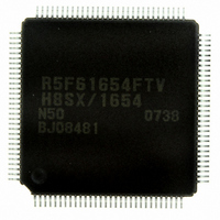
DF61654N50FTV Renesas Electronics America, DF61654N50FTV Datasheet - Page 277

DF61654N50FTV
Manufacturer Part Number
DF61654N50FTV
Description
IC H8SX/1654 MCU FLASH 120TQFP
Manufacturer
Renesas Electronics America
Series
H8® H8SX/1600r
Datasheet
1.DF61653N50FTV.pdf
(1020 pages)
Specifications of DF61654N50FTV
Core Processor
H8SX
Core Size
32-Bit
Speed
50MHz
Connectivity
I²C, IrDA, SCI, SmartCard, USB
Peripherals
DMA, PWM, WDT
Number Of I /o
75
Program Memory Size
512KB (512K x 8)
Program Memory Type
FLASH
Ram Size
40K x 8
Voltage - Supply (vcc/vdd)
3 V ~ 3.6 V
Data Converters
A/D 8x10b; D/A 2x8b
Oscillator Type
External
Operating Temperature
-20°C ~ 75°C
Package / Case
120-TQFP, 120-VQFP
For Use With
HS0005KCU11H - EMULATOR E10A-USB H8S(X),SH2(A)3DK1657 - DEV EVAL KIT FOR H8SX/1657
Lead Free Status / RoHS Status
Lead free / RoHS Compliant
Eeprom Size
-
Available stocks
Company
Part Number
Manufacturer
Quantity
Price
Company:
Part Number:
DF61654N50FTV
Manufacturer:
Renesas Electronics America
Quantity:
10 000
- Current page: 277 of 1020
- Download datasheet (6Mb)
6.15
In a reset, this LSI, including the bus controller, enters the reset state immediately, and any
executing bus cycle is aborted.
6.16
(1)
The BSC registers must be specified before accessing the external address space. In on-chip ROM
disabled mode, the BSC registers must be specified before accessing the external address space for
other than an instruction fetch access.
(2)
In this LSI, if the ACSE bit in MSTPCRA is set to 1, and then a SLEEP instruction is executed
with the setting for all peripheral module clocks to be stopped (MSTPCRA and MSTPCRB =
H'FFFFFFFF) or for operation of the 8-bit timer module alone (MSTPCRA and MSTPCRB =
H'F[E to 0]FFFFFF), and a transition is made to the sleep state, the all-module-clock-stop mode is
entered in which the clock is also stopped for the bus controller and I/O ports. For details, see
section 22, Power-Down Modes.
In this state, the external bus release function is halted. To use the external bus release function in
sleep mode, the ACSE bit in MSTPCR must be cleared to 0. Conversely, if a SLEEP instruction to
place the chip in all-module-clock-stop mode is executed in the external bus released state, the
transition to all-module-clock-stop mode is deferred and performed until after the bus is
recovered.
(3)
In this LSI, internal bus master operation does not stop even while the bus is released, as long as
the program is running in on-chip ROM, etc., and no external access occurs. If a SLEEP
instruction to place the chip in software standby mode is executed while the external bus is
released, the transition to software standby mode is deferred and performed after the bus is
recovered.
Also, since clock oscillation halts in software standby mode, if the BREQ signal goes low in this
mode, indicating an external bus release request, the request cannot be answered until the chip has
recovered from the software standby mode.
Note that the BACK and BREQO pins are both in the high-impedance state in software standby
mode.
Setting Registers
External Bus Release Function and All-Module-Clock-Stop Mode
External Bus Release Function and Software Standby
Bus Controller Operation in Reset
Usage Notes
Rev.1.00 Sep. 08, 2005 Page 227 of 966
Section 6 Bus Controller (BSC)
REJ09B0219-0100
Related parts for DF61654N50FTV
Image
Part Number
Description
Manufacturer
Datasheet
Request
R

Part Number:
Description:
KIT STARTER FOR M16C/29
Manufacturer:
Renesas Electronics America
Datasheet:

Part Number:
Description:
KIT STARTER FOR R8C/2D
Manufacturer:
Renesas Electronics America
Datasheet:

Part Number:
Description:
R0K33062P STARTER KIT
Manufacturer:
Renesas Electronics America
Datasheet:

Part Number:
Description:
KIT STARTER FOR R8C/23 E8A
Manufacturer:
Renesas Electronics America
Datasheet:

Part Number:
Description:
KIT STARTER FOR R8C/25
Manufacturer:
Renesas Electronics America
Datasheet:

Part Number:
Description:
KIT STARTER H8S2456 SHARPE DSPLY
Manufacturer:
Renesas Electronics America
Datasheet:

Part Number:
Description:
KIT STARTER FOR R8C38C
Manufacturer:
Renesas Electronics America
Datasheet:

Part Number:
Description:
KIT STARTER FOR R8C35C
Manufacturer:
Renesas Electronics America
Datasheet:

Part Number:
Description:
KIT STARTER FOR R8CL3AC+LCD APPS
Manufacturer:
Renesas Electronics America
Datasheet:

Part Number:
Description:
KIT STARTER FOR RX610
Manufacturer:
Renesas Electronics America
Datasheet:

Part Number:
Description:
KIT STARTER FOR R32C/118
Manufacturer:
Renesas Electronics America
Datasheet:

Part Number:
Description:
KIT DEV RSK-R8C/26-29
Manufacturer:
Renesas Electronics America
Datasheet:

Part Number:
Description:
KIT STARTER FOR SH7124
Manufacturer:
Renesas Electronics America
Datasheet:

Part Number:
Description:
KIT STARTER FOR H8SX/1622
Manufacturer:
Renesas Electronics America
Datasheet:

Part Number:
Description:
KIT DEV FOR SH7203
Manufacturer:
Renesas Electronics America
Datasheet:


