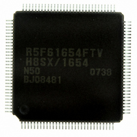
DF61654N50FTV Renesas Electronics America, DF61654N50FTV Datasheet - Page 35

DF61654N50FTV
Manufacturer Part Number
DF61654N50FTV
Description
IC H8SX/1654 MCU FLASH 120TQFP
Manufacturer
Renesas Electronics America
Series
H8® H8SX/1600r
Datasheet
1.DF61653N50FTV.pdf
(1020 pages)
Specifications of DF61654N50FTV
Core Processor
H8SX
Core Size
32-Bit
Speed
50MHz
Connectivity
I²C, IrDA, SCI, SmartCard, USB
Peripherals
DMA, PWM, WDT
Number Of I /o
75
Program Memory Size
512KB (512K x 8)
Program Memory Type
FLASH
Ram Size
40K x 8
Voltage - Supply (vcc/vdd)
3 V ~ 3.6 V
Data Converters
A/D 8x10b; D/A 2x8b
Oscillator Type
External
Operating Temperature
-20°C ~ 75°C
Package / Case
120-TQFP, 120-VQFP
For Use With
HS0005KCU11H - EMULATOR E10A-USB H8S(X),SH2(A)3DK1657 - DEV EVAL KIT FOR H8SX/1657
Lead Free Status / RoHS Status
Lead free / RoHS Compliant
Eeprom Size
-
Available stocks
Company
Part Number
Manufacturer
Quantity
Price
Company:
Part Number:
DF61654N50FTV
Manufacturer:
Renesas Electronics America
Quantity:
10 000
- Current page: 35 of 1020
- Download datasheet (6Mb)
Section 12 8-Bit Timers (TMR)
Figure 12.1 Block Diagram of 8-Bit Timer Module (Unit 0) ..................................................... 502
Figure 12.2 Block Diagram of 8-Bit Timer Module (Unit 1) ..................................................... 503
Figure 12.3 Block Diagram of 8-Bit Timer Module (Unit 2) ..................................................... 504
Figure 12.4 Block Diagram of 8-Bit Timer Module (Unit 3) ..................................................... 505
Figure 12.5 Example of Pulse Output......................................................................................... 519
Figure 12.6 Example of Reset Input ........................................................................................... 519
Figure 12.7 Count Timing for Internal Clock Input.................................................................... 520
Figure 12.8 Count Timing for External Clock Input .................................................................. 520
Figure 12.9 Timing of CMF Setting at Compare Match............................................................. 521
Figure 12.10 Timing of Toggled Timer Output at Compare Match A ....................................... 521
Figure 12.11 Timing of Counter Clear by Compare Match........................................................ 522
Figure 12.12 Timing of Clearance by External Reset (Rising Edge).......................................... 522
Figure 12.13 Timing of Clearance by External Reset (High Level) ........................................... 522
Figure 12.14 Timing of OVF Setting.......................................................................................... 523
Figure 12.15 Conflict between TCNT Write and Clear.............................................................. 526
Figure 12.16 Conflict between TCNT Write and Increment ...................................................... 527
Figure 12.17 Conflict between TCOR Write and Compare Match............................................. 527
Section 13 Watchdog Timer (WDT)
Figure 13.1 Block Diagram of WDT .......................................................................................... 532
Figure 13.2 Operation in Watchdog Timer Mode....................................................................... 537
Figure 13.3 Operation in Interval Timer Mode........................................................................... 538
Figure 13.4 Writing to TCNT, TCSR, and RSTCSR.................................................................. 539
Figure 13.5 Conflict between TCNT Write and Increment ........................................................ 540
Figure 13.6 Circuit for System Reset by WDTOVF Signal (Example)...................................... 541
Section 14 Serial Communication Interface (SCI, IrDA, CRC)
Figure 14.1 Block Diagram of SCI_0, 1, 2, and 4 ...................................................................... 546
Figure 14.2 Block Diagram of SCI_5 and SCI_6 ....................................................................... 547
Figure 14.3 Examples of Base Clock when Average Transfer Rate Is Selected (1) ................... 581
Figure 14.3 Examples of Base Clock when Average Transfer Rate Is Selected (2) ................... 582
Figure 14.3 Examples of Base Clock when Average Transfer Rate Is Selected (3) ................... 583
Figure 14.4 Example of Average Transfer Rate Setting when TMR Clock Is Input .................. 584
Figure 14.5 Data Format in Asynchronous Communication
(Example with 8-Bit Data, Parity, Two Stop Bits) ................................................. 586
Figure 14.6 Receive Data Sampling Timing in Asynchronous Mode ........................................ 588
Figure 14.7 Phase Relation between Output Clock and Transmit Data
(Asynchronous Mode) ............................................................................................. 589
Figure 14.8 Sample SCI Initialization Flowchart ....................................................................... 590
Rev.1.00 Sep. 08, 2005 Page xxxiii of xlviii
Related parts for DF61654N50FTV
Image
Part Number
Description
Manufacturer
Datasheet
Request
R

Part Number:
Description:
KIT STARTER FOR M16C/29
Manufacturer:
Renesas Electronics America
Datasheet:

Part Number:
Description:
KIT STARTER FOR R8C/2D
Manufacturer:
Renesas Electronics America
Datasheet:

Part Number:
Description:
R0K33062P STARTER KIT
Manufacturer:
Renesas Electronics America
Datasheet:

Part Number:
Description:
KIT STARTER FOR R8C/23 E8A
Manufacturer:
Renesas Electronics America
Datasheet:

Part Number:
Description:
KIT STARTER FOR R8C/25
Manufacturer:
Renesas Electronics America
Datasheet:

Part Number:
Description:
KIT STARTER H8S2456 SHARPE DSPLY
Manufacturer:
Renesas Electronics America
Datasheet:

Part Number:
Description:
KIT STARTER FOR R8C38C
Manufacturer:
Renesas Electronics America
Datasheet:

Part Number:
Description:
KIT STARTER FOR R8C35C
Manufacturer:
Renesas Electronics America
Datasheet:

Part Number:
Description:
KIT STARTER FOR R8CL3AC+LCD APPS
Manufacturer:
Renesas Electronics America
Datasheet:

Part Number:
Description:
KIT STARTER FOR RX610
Manufacturer:
Renesas Electronics America
Datasheet:

Part Number:
Description:
KIT STARTER FOR R32C/118
Manufacturer:
Renesas Electronics America
Datasheet:

Part Number:
Description:
KIT DEV RSK-R8C/26-29
Manufacturer:
Renesas Electronics America
Datasheet:

Part Number:
Description:
KIT STARTER FOR SH7124
Manufacturer:
Renesas Electronics America
Datasheet:

Part Number:
Description:
KIT STARTER FOR H8SX/1622
Manufacturer:
Renesas Electronics America
Datasheet:

Part Number:
Description:
KIT DEV FOR SH7203
Manufacturer:
Renesas Electronics America
Datasheet:


