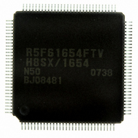
DF61654N50FTV Renesas Electronics America, DF61654N50FTV Datasheet - Page 757

DF61654N50FTV
Manufacturer Part Number
DF61654N50FTV
Description
IC H8SX/1654 MCU FLASH 120TQFP
Manufacturer
Renesas Electronics America
Series
H8® H8SX/1600r
Datasheet
1.DF61653N50FTV.pdf
(1020 pages)
Specifications of DF61654N50FTV
Core Processor
H8SX
Core Size
32-Bit
Speed
50MHz
Connectivity
I²C, IrDA, SCI, SmartCard, USB
Peripherals
DMA, PWM, WDT
Number Of I /o
75
Program Memory Size
512KB (512K x 8)
Program Memory Type
FLASH
Ram Size
40K x 8
Voltage - Supply (vcc/vdd)
3 V ~ 3.6 V
Data Converters
A/D 8x10b; D/A 2x8b
Oscillator Type
External
Operating Temperature
-20°C ~ 75°C
Package / Case
120-TQFP, 120-VQFP
For Use With
HS0005KCU11H - EMULATOR E10A-USB H8S(X),SH2(A)3DK1657 - DEV EVAL KIT FOR H8SX/1657
Lead Free Status / RoHS Status
Lead free / RoHS Compliant
Eeprom Size
-
Available stocks
Company
Part Number
Manufacturer
Quantity
Price
Company:
Part Number:
DF61654N50FTV
Manufacturer:
Renesas Electronics America
Quantity:
10 000
- Current page: 757 of 1020
- Download datasheet (6Mb)
16.3.1
ICCRA enables or disables I
master or slave mode, transmission or reception, and transfer clock frequency in master mode.
Bit
7
6
5
4
3
2
1
0
Bit
Bit Name
Initial Value
R/W
I
2
Bit Name
ICE
RCVD
MST
TRS
CKS3
CKS2
CKS1
CKS0
C Bus Control Register A (ICCRA)
R/W
ICE
7
0
Initial
Value
0
0
0
0
0
0
0
0
RCVD
R/W
6
0
2
C bus interface, controls transmission or reception, and selects
R/W
R/W
R/W
R/W
R/W
R/W
R/W
R/W
R/W
MST
R/W
5
0
Description
I
0: This module is halted
1: This bit is enabled for transfer operations (SCL and
Reception Disable
This bit enables or disables the next operation when
TRS is 0 and ICDRR is read.
0: Enables next reception
1: Disables next reception
Master/Slave Select
Transmit/Receive Select
When arbitration is lost in master mode, MST and
TRS are both reset by hardware, causing a transition
to slave receive mode. Modification of the TRS bit
should be made between transfer frames.
Operating modes are described below according to
MST and TRS combination.
00: Slave receive mode
01: Slave transmit mode
10: Master receive mode
11: Master transmit mode
Transfer Clock Select 3 to 0
These bits are valid only in master mode. Make
setting according to the required transfer rate. For
details on the transfer rate, see Table 16.2.
2
C Bus Interface Enable
SDA pins are bus drive state)
TRS
R/W
4
0
CKS3
R/W
3
0
Rev.1.00 Sep. 08, 2005 Page 707 of 966
Section 16 I
CKS2
R/W
2
0
2
C Bus Interface2 (IIC2)
CKS1
R/W
1
0
REJ09B0219-0100
CKS0
R/W
0
0
Related parts for DF61654N50FTV
Image
Part Number
Description
Manufacturer
Datasheet
Request
R

Part Number:
Description:
KIT STARTER FOR M16C/29
Manufacturer:
Renesas Electronics America
Datasheet:

Part Number:
Description:
KIT STARTER FOR R8C/2D
Manufacturer:
Renesas Electronics America
Datasheet:

Part Number:
Description:
R0K33062P STARTER KIT
Manufacturer:
Renesas Electronics America
Datasheet:

Part Number:
Description:
KIT STARTER FOR R8C/23 E8A
Manufacturer:
Renesas Electronics America
Datasheet:

Part Number:
Description:
KIT STARTER FOR R8C/25
Manufacturer:
Renesas Electronics America
Datasheet:

Part Number:
Description:
KIT STARTER H8S2456 SHARPE DSPLY
Manufacturer:
Renesas Electronics America
Datasheet:

Part Number:
Description:
KIT STARTER FOR R8C38C
Manufacturer:
Renesas Electronics America
Datasheet:

Part Number:
Description:
KIT STARTER FOR R8C35C
Manufacturer:
Renesas Electronics America
Datasheet:

Part Number:
Description:
KIT STARTER FOR R8CL3AC+LCD APPS
Manufacturer:
Renesas Electronics America
Datasheet:

Part Number:
Description:
KIT STARTER FOR RX610
Manufacturer:
Renesas Electronics America
Datasheet:

Part Number:
Description:
KIT STARTER FOR R32C/118
Manufacturer:
Renesas Electronics America
Datasheet:

Part Number:
Description:
KIT DEV RSK-R8C/26-29
Manufacturer:
Renesas Electronics America
Datasheet:

Part Number:
Description:
KIT STARTER FOR SH7124
Manufacturer:
Renesas Electronics America
Datasheet:

Part Number:
Description:
KIT STARTER FOR H8SX/1622
Manufacturer:
Renesas Electronics America
Datasheet:

Part Number:
Description:
KIT DEV FOR SH7203
Manufacturer:
Renesas Electronics America
Datasheet:


