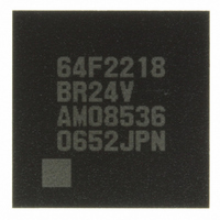
DF2218BR24V Renesas Electronics America, DF2218BR24V Datasheet - Page 128

DF2218BR24V
Manufacturer Part Number
DF2218BR24V
Description
IC H8S/2218 MCU FLASH 112-LFBGA
Manufacturer
Renesas Electronics America
Series
H8® H8S/2200r
Specifications of DF2218BR24V
Core Processor
H8S/2000
Core Size
16-Bit
Speed
24MHz
Connectivity
SCI, SmartCard, USB
Peripherals
DMA, POR, PWM, WDT
Number Of I /o
69
Program Memory Size
128KB (128K x 8)
Program Memory Type
FLASH
Ram Size
12K x 8
Voltage - Supply (vcc/vdd)
2.7 V ~ 3.6 V
Data Converters
A/D 6x10b
Oscillator Type
External
Operating Temperature
-20°C ~ 75°C
Package / Case
112-LFBGA
For Use With
HS0005KCU11H - EMULATOR E10A-USB H8S(X),SH2(A)3DK2218-SS - KIT DEV H8S/2218 WINDOWS SIDESHW3DK2218 - DEV EVAL KIT H8S/2218
Lead Free Status / RoHS Status
Lead free / RoHS Compliant
Eeprom Size
-
Available stocks
Company
Part Number
Manufacturer
Quantity
Price
Company:
Part Number:
DF2218BR24V
Manufacturer:
Renesas Electronics America
Quantity:
10 000
- Current page: 128 of 758
- Download datasheet (5Mb)
3.2
The following registers are related to the operating mode.
• Mode control register (MDCR)
• System control register (SYSCR)
3.2.1
MDCR is used to monitor the current operating mode of this LSI. MDCR should not be modified.
Notes: 1. Determined by the FWE and MD2 to MD0 pin settings.
3.2.2
SYSCR is used to select the interrupt control mode and the detected edge for NMI, select the
MRES input pin* enable or disable, and enables or disables on-chip RAM.
Rev.7.00 Dec. 24, 2008 Page 72 of 698
REJ09B0074-0700
Bit
7 to 4
3
2
1
0
2. Supported only by the H8S/2218 Group.
Bit Name
⎯
FWE
MDS2
MDS1
MDS0
Mode Control Register (MDCR)
System Control Register (SYSCR)
Register Descriptions
Initial Value R/W
Undefined
⎯*
⎯*
⎯*
⎯*
1
1
1
1
⎯
R
R
R
R
Description
Reserved
These bits are always read as undefined value and
cannot be modified.
Flash Programming Enable
Reflects the input level at the FWE pin. This bit
functions same as the FWE bit in the FLMCR1
register.
Mode Select 2 to 0
These bits indicate the input levels at pins MD2 to
MD0 (the current operating mode). Bits MDS2 to
MDS0 correspond to MD2 to MD0. MDS2 to MDS0
are read-only bits and they cannot be written to. The
mode pin (MD2 to MD0) input levels are latched into
these bits when MDCR is read.
These latches are canceled by a power-on reset, but
maintained at manual reset*
2
.
Related parts for DF2218BR24V
Image
Part Number
Description
Manufacturer
Datasheet
Request
R

Part Number:
Description:
CONN SOCKET 2POS 7.92MM WHITE
Manufacturer:
Hirose Electric Co Ltd
Datasheet:

Part Number:
Description:
CONN SOCKET 4POS 7.92MM WHITE
Manufacturer:
Hirose Electric Co Ltd
Datasheet:

Part Number:
Description:
CONN SOCKET 5POS 7.92MM WHITE
Manufacturer:
Hirose Electric Co Ltd
Datasheet:

Part Number:
Description:
CONN SOCKET 3POS 7.92MM WHITE
Manufacturer:
Hirose Electric Co Ltd
Datasheet:

Part Number:
Description:
CONN SOCKET 5POS 7.92MM WHITE
Manufacturer:
Hirose Electric Co Ltd
Datasheet:

Part Number:
Description:
CONN SOCKET 2POS 7.92MM WHITE
Manufacturer:
Hirose Electric Co Ltd
Datasheet:

Part Number:
Description:
CONN SOCKET 3POS 7.92MM WHITE
Manufacturer:
Hirose Electric Co Ltd
Datasheet:

Part Number:
Description:
CONN SOCKET 4POS 7.92MM WHITE
Manufacturer:
Hirose Electric Co Ltd
Datasheet:

Part Number:
Description:
CONN HEADER 2POS 7.92MM R/A TIN
Manufacturer:
Hirose Electric Co Ltd
Datasheet:

Part Number:
Description:
CONN HEADER 4POS 7.92MM R/A TIN
Manufacturer:
Hirose Electric Co Ltd
Datasheet:

Part Number:
Description:
KIT STARTER FOR M16C/29
Manufacturer:
Renesas Electronics America
Datasheet:

Part Number:
Description:
KIT STARTER FOR R8C/2D
Manufacturer:
Renesas Electronics America
Datasheet:

Part Number:
Description:
R0K33062P STARTER KIT
Manufacturer:
Renesas Electronics America
Datasheet:

Part Number:
Description:
KIT STARTER FOR R8C/23 E8A
Manufacturer:
Renesas Electronics America
Datasheet:

Part Number:
Description:
KIT STARTER FOR R8C/25
Manufacturer:
Renesas Electronics America
Datasheet:


