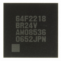
DF2218BR24V Renesas Electronics America, DF2218BR24V Datasheet - Page 657

DF2218BR24V
Manufacturer Part Number
DF2218BR24V
Description
IC H8S/2218 MCU FLASH 112-LFBGA
Manufacturer
Renesas Electronics America
Series
H8® H8S/2200r
Specifications of DF2218BR24V
Core Processor
H8S/2000
Core Size
16-Bit
Speed
24MHz
Connectivity
SCI, SmartCard, USB
Peripherals
DMA, POR, PWM, WDT
Number Of I /o
69
Program Memory Size
128KB (128K x 8)
Program Memory Type
FLASH
Ram Size
12K x 8
Voltage - Supply (vcc/vdd)
2.7 V ~ 3.6 V
Data Converters
A/D 6x10b
Oscillator Type
External
Operating Temperature
-20°C ~ 75°C
Package / Case
112-LFBGA
For Use With
HS0005KCU11H - EMULATOR E10A-USB H8S(X),SH2(A)3DK2218-SS - KIT DEV H8S/2218 WINDOWS SIDESHW3DK2218 - DEV EVAL KIT H8S/2218
Lead Free Status / RoHS Status
Lead free / RoHS Compliant
Eeprom Size
-
Available stocks
Company
Part Number
Manufacturer
Quantity
Price
Company:
Part Number:
DF2218BR24V
Manufacturer:
Renesas Electronics America
Quantity:
10 000
- Current page: 657 of 758
- Download datasheet (5Mb)
19.2.2
An external clock signal can be input as shown in an example in figure 19.4. If the XTAL pin is
left open, make sure that stray capacitance is no more than 10 pF. When complementary clock
input to XTAL pin, the external clock input should be fixed high in standby mode, subactive
mode, subsleep mode, or watch mode.
Table 19.3 shows the input conditions for the external clock.
Table 19.3 External Clock Input Conditions
The external clock input conditions when the duty adjustment circuit is not used are shown in table
19.4. When the duty adjustment circuit is not used, note that the maximum operating frequency
depends on the external clock input waveform. For example, if t
= 5.25 ns, the maximum operating frequency becomes 19.2 MHz depending on the clcok cycle
time of 52.1 ns.
Item
External clock input low pulse width
External clock input high pulse width
External clock rise time
External clock fall time
Clock low pulse width level
Clock high pulse width level
Inputting External Clock
Figure 19.4 External Clock Input (Examples)
EXTAL
XTAL
EXTAL
XTAL
Symbol
t
t
t
t
t
t
EXL
EXH
EXr
EXf
CL
CH
(b) Complementary clock input at XTAL pin
min
65
65
—
—
0.35
0.35
VCC= 2.4 to 3.6V
(a) XTAL pin left open
max
—
—
15
15
0.65
0.65
Open
Min
25
25
—
—
0.4
0.4
VCC = 2.7 to 3.6V
Rev.7.00 Dec. 24, 2008 Page 601 of 698
External clock input
External clock input
max
—
—
6.25
6.25
0.6
0.6
EXL
min
15.5
15.5
—
—
0.4
0.4
= t
VCC = 3.0 to 3.6V
EXH
= 20.8 ns and t
max
—
—
5.25
5.25
0.6
0.6
REJ09B0074-0700
Unit
ns
ns
ns
ns
tcyc
tcyc
Test
Conditions
Figure 19.5
Figure 22.3
EXr
= t
EXf
Related parts for DF2218BR24V
Image
Part Number
Description
Manufacturer
Datasheet
Request
R

Part Number:
Description:
CONN SOCKET 2POS 7.92MM WHITE
Manufacturer:
Hirose Electric Co Ltd
Datasheet:

Part Number:
Description:
CONN SOCKET 4POS 7.92MM WHITE
Manufacturer:
Hirose Electric Co Ltd
Datasheet:

Part Number:
Description:
CONN SOCKET 5POS 7.92MM WHITE
Manufacturer:
Hirose Electric Co Ltd
Datasheet:

Part Number:
Description:
CONN SOCKET 3POS 7.92MM WHITE
Manufacturer:
Hirose Electric Co Ltd
Datasheet:

Part Number:
Description:
CONN SOCKET 5POS 7.92MM WHITE
Manufacturer:
Hirose Electric Co Ltd
Datasheet:

Part Number:
Description:
CONN SOCKET 2POS 7.92MM WHITE
Manufacturer:
Hirose Electric Co Ltd
Datasheet:

Part Number:
Description:
CONN SOCKET 3POS 7.92MM WHITE
Manufacturer:
Hirose Electric Co Ltd
Datasheet:

Part Number:
Description:
CONN SOCKET 4POS 7.92MM WHITE
Manufacturer:
Hirose Electric Co Ltd
Datasheet:

Part Number:
Description:
CONN HEADER 2POS 7.92MM R/A TIN
Manufacturer:
Hirose Electric Co Ltd
Datasheet:

Part Number:
Description:
CONN HEADER 4POS 7.92MM R/A TIN
Manufacturer:
Hirose Electric Co Ltd
Datasheet:

Part Number:
Description:
KIT STARTER FOR M16C/29
Manufacturer:
Renesas Electronics America
Datasheet:

Part Number:
Description:
KIT STARTER FOR R8C/2D
Manufacturer:
Renesas Electronics America
Datasheet:

Part Number:
Description:
R0K33062P STARTER KIT
Manufacturer:
Renesas Electronics America
Datasheet:

Part Number:
Description:
KIT STARTER FOR R8C/23 E8A
Manufacturer:
Renesas Electronics America
Datasheet:

Part Number:
Description:
KIT STARTER FOR R8C/25
Manufacturer:
Renesas Electronics America
Datasheet:


