IPR-PCIE/1 Altera, IPR-PCIE/1 Datasheet - Page 234

IPR-PCIE/1
Manufacturer Part Number
IPR-PCIE/1
Description
IP CORE Renewal Of IP-PCIE/1
Manufacturer
Altera
Type
MegaCorer
Specifications of IPR-PCIE/1
Software Application
IP CORE, Interface And Protocols, PCI
Supported Families
Arria GX, Cyclone II, HardCopy II, Stratix II
Core Architecture
FPGA
Core Sub-architecture
Arria, Cyclone, Stratix
Rohs Compliant
NA
Function
PCI Express Compiler, x1 Link Width
License
Renewal License
Lead Free Status / RoHS Status
na
Lead Free Status / RoHS Status
na
- Current page: 234 of 362
- Download datasheet (7Mb)
15–6
Table 15–3. Testbench Verilog HDL Parameters for the Root Port Testbench
Chaining DMA Design Example
PCI Express Compiler User Guide
PIPE_MODE_SIM
NUM_CONNECTED_LANES
FAST_COUNTERS
Parameter
The testbench has several Verilog HDL parameters that control the overall operation
of the testbench. These parameters are described in
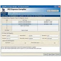
This design example shows how to use the MegaWizard Plug-In Manager flow to
create a chaining DMA native endpoint which supports simultaneous DMA read and
write transactions. The write DMA module implements write operations from the
endpoint memory to the root complex (RC) memory. The read DMA implements read
operations from the RC memory to the endpoint memory.
When operating on a hardware platform, the DMA is typically controlled by a
software application running on the root complex processor. In simulation, the
testbench generated by the PCI Express Compiler, along with this design example,
provides a BFM driver module in Verilog HDL or VHDL that controls the DMA
operations. Because the example relies on no other hardware interface than the PCI
Express link, you can use the design example for the initial hardware validation of
your system.
The design example includes the following two main components:
■
■
When using the MegaWizard Plug-In manager flow, both components are
automatically generated along with a testbench. All of the components are generated
in the language (Verilog HDL or VHDL) that you selected for the variation file.
The IP core variation
An application layer design example
0 or 1
1,2,4,8
0 or 1
Allowed
Values
Default
Value
1
8
1
Selects the PIPE interface (PIPE_MODE_SIM=1) or the serial
interface (PIPE_MODE_SIM= 0) for the simulation. The PIPE
interface typically simulates much faster than the serial
interface. If the variation name file only implements the PIPE
interface, then setting PIPE_MODE_SIM to 0 has no effect and
the PIPE interface is always used.
Controls how many lanes are interconnected by the testbench.
Setting this generic value to a lower number simulates the
endpoint operating on a narrower PCI Express interface than
the maximum.
If your variation only implements the ×1 IP core, then this
setting has no effect and only one lane is used.
Setting this parameter to a 1 speeds up simulation by making
many of the timing counters in the PCI Express IP core operate
faster than specified in the PCI Express specification.This
parameter should usually be set to 1, but can be set to 0 if there
is a need to simulate the true time-out values.
Table
Description
Chapter 15: Testbench and Design Example
15–3.
December 2010 Altera Corporation
Chaining DMA Design Example
Related parts for IPR-PCIE/1
Image
Part Number
Description
Manufacturer
Datasheet
Request
R

Part Number:
Description:
IP CORE Renewal Of IP-PCI/MT32
Manufacturer:
Altera
Datasheet:

Part Number:
Description:
IP CORE Renewal Of IP-PCI/MT64
Manufacturer:
Altera
Datasheet:

Part Number:
Description:
IP CORE Renewal Of IP-PCI/T32
Manufacturer:
Altera
Datasheet:

Part Number:
Description:
IP CORE Renewal Of IP-PCI/T64
Manufacturer:
Altera
Datasheet:

Part Number:
Description:
IP CORE Renewal Of IP-PCIE/4
Manufacturer:
Altera
Datasheet:

Part Number:
Description:
IP CORE Renewal Of IP-PCIE/8
Manufacturer:
Altera
Datasheet:

Part Number:
Description:
IP NIOS II MEGACORE RENEW
Manufacturer:
Altera
Datasheet:

Part Number:
Description:
IP CORE Renewal Of IP-XAUIPCS
Manufacturer:
Altera
Datasheet:

Part Number:
Description:
CPLD, EP610 Family, ECMOS Process, 300 Gates, 16 Macro Cells, 16 Reg., 16 User I/Os, 5V Supply, 35 Speed Grade, 24DIP
Manufacturer:
Altera Corporation
Datasheet:

Part Number:
Description:
CPLD, EP610 Family, ECMOS Process, 300 Gates, 16 Macro Cells, 16 Reg., 16 User I/Os, 5V Supply, 15 Speed Grade, 24DIP
Manufacturer:
Altera Corporation
Datasheet:

Part Number:
Description:
Manufacturer:
Altera Corporation
Datasheet:


