IPR-PCIE/1 Altera, IPR-PCIE/1 Datasheet - Page 49
IPR-PCIE/1
Manufacturer Part Number
IPR-PCIE/1
Description
IP CORE Renewal Of IP-PCIE/1
Manufacturer
Altera
Type
MegaCorer
Specifications of IPR-PCIE/1
Software Application
IP CORE, Interface And Protocols, PCI
Supported Families
Arria GX, Cyclone II, HardCopy II, Stratix II
Core Architecture
FPGA
Core Sub-architecture
Arria, Cyclone, Stratix
Rohs Compliant
NA
Function
PCI Express Compiler, x1 Link Width
License
Renewal License
Lead Free Status / RoHS Status
na
Lead Free Status / RoHS Status
na


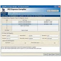
Chapter 3: Parameter Settings
Capabilities Parameters
Table 3–3. Capabilities Parameters (Part 1 of 4)
December 2010 Altera Corporation
Tags supported
Implement
completion timeout
disable
0x0A8
Completion
timeout range
Parameter
1
The Capabilities page that appears in SOPC Builder does not include the Simulation
Mode and Summary tabs.
4–256
On/Off
Ranges A–D
Value
Indicates the number of tags supported for non-posted requests transmitted by the
application layer. The following options are available:
This parameter sets the values in the Device Control register (0x088) of the PCI
Express capability structure described in
The transaction layer tracks all outstanding completions for non-posted requests
made by the application. This parameter configures the transaction layer for the
maximum number to track. The application layer must set the tag values in all
non-posted PCI Express headers to be less than this value. Values greater than 32
also set the extended tag field supported bit in the configuration space device
capabilities register. The application can only use tag numbers greater than 31 if
configuration software sets the extended tag field enable bit of the device control
register. This bit is available to the application as cfg_devcsr[8].
This option is only selectable for PCI Express version 2.0 and higher root ports . For
PCI Express version 2.0 and higher endpoints this option is forced to On. For PCI
Express version 1.0a and 1.1 variations, this option is forced to Off. The timeout
range is selectable. When On, the core supports the completion timeout disable
mechanism via the PCI Express Device Control Register 2. The application layer logic
must implement the actual completion timeout mechanism for the required ranges.
This option is only available for PCI Express version 2.0 and higher. It indicates
device function support for the optional completion timeout programmability
mechanism. This mechanism allows system software to modify the completion
timeout value. This field is applicable only to root ports and endpoints that issue
requests on their own behalf. Completion timeouts are specified and enabled via the
Device Control 2 register (0x0A8) of the PCI Express Capability Structure Version 2.0
described in
must be hardwired to 0x0000b. Four time value ranges are defined:
Bits are set according to the table below to show timeout value ranges supported.
0x0000b completion timeout programming is not supported and the function must
implement a timeout value in the range 50 s to 50 ms. The following encodings are
used to specify the range:
Hard IP: 32 or 64 tags for ×1, ×4, and ×8
Soft IP: 4–256 tags for ×1 and ×4; 4–32 for ×8
SOPC Builder: 16 tags for ×1 and ×4
Range A: 50 µs to 10 ms
Range B: 10 ms to 250 ms
Range C: 250 ms to 4 s
Range D: 4 s to 64 s
Device Capabilities
Table 6–8 on page
0x084
6–5. For all other functions this field is reserved and
Description
Table 6–7 on page
PCI Express Compiler User Guide
6–4.
3–7
Related parts for IPR-PCIE/1
Image
Part Number
Description
Manufacturer
Datasheet
Request
R

Part Number:
Description:
IP CORE Renewal Of IP-PCI/MT32
Manufacturer:
Altera
Datasheet:
Part Number:
Description:
IP CORE Renewal Of IP-PCI/MT64
Manufacturer:
Altera
Datasheet:
Part Number:
Description:
IP CORE Renewal Of IP-PCI/T32
Manufacturer:
Altera
Datasheet:
Part Number:
Description:
IP CORE Renewal Of IP-PCI/T64
Manufacturer:
Altera
Datasheet:

Part Number:
Description:
IP CORE Renewal Of IP-PCIE/4
Manufacturer:
Altera
Datasheet:
Part Number:
Description:
IP CORE Renewal Of IP-PCIE/8
Manufacturer:
Altera
Datasheet:
Part Number:
Description:
IP NIOS II MEGACORE RENEW
Manufacturer:
Altera
Datasheet:
Part Number:
Description:
IP CORE Renewal Of IP-XAUIPCS
Manufacturer:
Altera
Datasheet:

Part Number:
Description:
CPLD, EP610 Family, ECMOS Process, 300 Gates, 16 Macro Cells, 16 Reg., 16 User I/Os, 5V Supply, 35 Speed Grade, 24DIP
Manufacturer:
Altera Corporation
Datasheet:
Part Number:
Description:
CPLD, EP610 Family, ECMOS Process, 300 Gates, 16 Macro Cells, 16 Reg., 16 User I/Os, 5V Supply, 15 Speed Grade, 24DIP
Manufacturer:
Altera Corporation
Datasheet:
Part Number:
Description:
Manufacturer:
Altera Corporation
Datasheet: