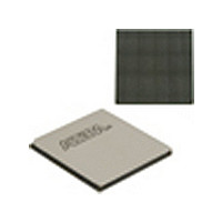
EP4SGX530HH35C2N Altera, EP4SGX530HH35C2N Datasheet - Page 158

EP4SGX530HH35C2N
Manufacturer Part Number
EP4SGX530HH35C2N
Description
IC STRATIX IV FPGA 530K 1152HBGA
Manufacturer
Altera
Series
Stratix® IV GXr
Datasheets
1.EP4SGX110DF29C3N.pdf
(80 pages)
2.EP4SGX110DF29C3N.pdf
(1154 pages)
3.EP4SGX110DF29C3N.pdf
(432 pages)
4.EP4SGX110DF29C3N.pdf
(22 pages)
5.EP4SGX110DF29C3N.pdf
(30 pages)
6.EP4SGX110DF29C3N.pdf
(72 pages)
7.EP4SGX530HH35C2N.pdf
(1145 pages)
Specifications of EP4SGX530HH35C2N
Number Of Logic Elements/cells
531200
Number Of Labs/clbs
21248
Total Ram Bits
27376
Number Of I /o
564
Voltage - Supply
0.87 V ~ 0.93 V
Mounting Type
Surface Mount
Operating Temperature
0°C ~ 85°C
Package / Case
1152-HBGA
Family Name
Stratix® IV
Number Of Logic Blocks/elements
531200
# Registers
424960
# I/os (max)
560
Process Technology
40nm
Operating Supply Voltage (typ)
900mV
Logic Cells
531200
Ram Bits
28033024
Operating Supply Voltage (min)
0.87V
Operating Supply Voltage (max)
0.93V
Operating Temp Range
0C to 85C
Operating Temperature Classification
Commercial
Mounting
Surface Mount
Pin Count
1152
Package Type
FCHBGA
Lead Free Status / RoHS Status
Lead free / RoHS Compliant
Number Of Gates
-
Lead Free Status / Rohs Status
Compliant
Available stocks
Company
Part Number
Manufacturer
Quantity
Price
- EP4SGX110DF29C3N PDF datasheet
- EP4SGX110DF29C3N PDF datasheet #2
- EP4SGX110DF29C3N PDF datasheet #3
- EP4SGX110DF29C3N PDF datasheet #4
- EP4SGX110DF29C3N PDF datasheet #5
- EP4SGX110DF29C3N PDF datasheet #6
- EP4SGX530HH35C2N PDF datasheet #7
- Current page: 158 of 432
- Download datasheet (11Mb)
5–42
Stratix IV Device Handbook Volume 1
f
Manual Clock Switchover
In manual clock switchover mode, the clkswitch signal controls whether inclk0 or
inclk1 is selected as the input clock to the PLL. By default, inclk0 is selected. A
low-to-high transition on clkswitch and clkswitch being held high for at least three
inclk cycles initiates a clock switchover event. You must bring clkswitch back low
again in order to perform another switchover event in the future. If you do not require
another switchover event in the future, you can leave clkswitch in a logic high state
after the initial switch. Pulsing clkswitch high for at least three inclk cycles performs
another switchover event. If inclk0 and inclk1 are different frequencies and are
always running, the clkswitch minimum high time must be greater than or equal to
three of the slower frequency inclk0 or inclk1 cycles.
diagram of the manual switchover circuit.
Figure 5–37. Manual Clock Switchover Circuitry in Stratix IV PLLs
For more information about PLL software support in the Quartus II software, refer to
the
Guidelines
When implementing clock switchover in Stratix IV PLLs, use the following
guidelines:
■
■
■
Automatic clock switchover requires that the inclk0 and inclk1 frequencies be
within 100% (2×) of each other. Failing to meet this requirement causes the
clkbad[0] and clkbad[1] signals to not function properly.
When using manual clock switchover, the difference between inclk0 and inclk1
can be more than 100% (2×). However, differences in frequency, phase, or both, of
the two clock sources will likely cause the PLL to lose lock. Resetting the PLL
ensures that the correct phase relationships are maintained between the input and
output clocks.
1
Applications that require a clock switchover feature and a small frequency drift
must use a low-bandwidth PLL. The low-bandwidth PLL reacts more slowly than
a high-bandwidth PLL to reference input clock changes. When switchover
happens, a low-bandwidth PLL propagates the stopping of the clock to the output
more slowly than a high-bandwidth PLL. However, be aware that the
low-bandwidth PLL also increases lock time.
Phase-Locked Loop (ALTPLL) Megafunction User
clkswitch
inclk0
inclk1
Both inclk0 and inclk1 must be running when the clkswitch signal goes
high to initiate the manual clock switchover event. Failing to meet this
requirement causes the clock switchover to not function properly.
Control Logic
Clock Switch
muxout
n Counter
Chapter 5: Clock Networks and PLLs in Stratix IV Devices
refclk
Guide.
Figure 5–37
February 2011 Altera Corporation
PFD
shows a block
PLLs in Stratix IV Devices
fbclk
Related parts for EP4SGX530HH35C2N
Image
Part Number
Description
Manufacturer
Datasheet
Request
R

Part Number:
Description:
CYCLONE II STARTER KIT EP2C20N
Manufacturer:
Altera
Datasheet:

Part Number:
Description:
CPLD, EP610 Family, ECMOS Process, 300 Gates, 16 Macro Cells, 16 Reg., 16 User I/Os, 5V Supply, 35 Speed Grade, 24DIP
Manufacturer:
Altera Corporation
Datasheet:

Part Number:
Description:
CPLD, EP610 Family, ECMOS Process, 300 Gates, 16 Macro Cells, 16 Reg., 16 User I/Os, 5V Supply, 15 Speed Grade, 24DIP
Manufacturer:
Altera Corporation
Datasheet:

Part Number:
Description:
Manufacturer:
Altera Corporation
Datasheet:

Part Number:
Description:
CPLD, EP610 Family, ECMOS Process, 300 Gates, 16 Macro Cells, 16 Reg., 16 User I/Os, 5V Supply, 30 Speed Grade, 24DIP
Manufacturer:
Altera Corporation
Datasheet:

Part Number:
Description:
High-performance, low-power erasable programmable logic devices with 8 macrocells, 10ns
Manufacturer:
Altera Corporation
Datasheet:

Part Number:
Description:
High-performance, low-power erasable programmable logic devices with 8 macrocells, 7ns
Manufacturer:
Altera Corporation
Datasheet:

Part Number:
Description:
Classic EPLD
Manufacturer:
Altera Corporation
Datasheet:

Part Number:
Description:
High-performance, low-power erasable programmable logic devices with 8 macrocells, 10ns
Manufacturer:
Altera Corporation
Datasheet:

Part Number:
Description:
Manufacturer:
Altera Corporation
Datasheet:

Part Number:
Description:
Manufacturer:
Altera Corporation
Datasheet:

Part Number:
Description:
Manufacturer:
Altera Corporation
Datasheet:

Part Number:
Description:
CPLD, EP610 Family, ECMOS Process, 300 Gates, 16 Macro Cells, 16 Reg., 16 User I/Os, 5V Supply, 25 Speed Grade, 24DIP
Manufacturer:
Altera Corporation
Datasheet:


