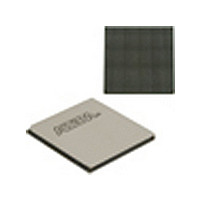
EP4SGX530HH35C2N Altera, EP4SGX530HH35C2N Datasheet - Page 222

EP4SGX530HH35C2N
Manufacturer Part Number
EP4SGX530HH35C2N
Description
IC STRATIX IV FPGA 530K 1152HBGA
Manufacturer
Altera
Series
Stratix® IV GXr
Datasheets
1.EP4SGX110DF29C3N.pdf
(80 pages)
2.EP4SGX110DF29C3N.pdf
(1154 pages)
3.EP4SGX110DF29C3N.pdf
(432 pages)
4.EP4SGX110DF29C3N.pdf
(22 pages)
5.EP4SGX110DF29C3N.pdf
(30 pages)
6.EP4SGX110DF29C3N.pdf
(72 pages)
7.EP4SGX530HH35C2N.pdf
(1145 pages)
Specifications of EP4SGX530HH35C2N
Number Of Logic Elements/cells
531200
Number Of Labs/clbs
21248
Total Ram Bits
27376
Number Of I /o
564
Voltage - Supply
0.87 V ~ 0.93 V
Mounting Type
Surface Mount
Operating Temperature
0°C ~ 85°C
Package / Case
1152-HBGA
Family Name
Stratix® IV
Number Of Logic Blocks/elements
531200
# Registers
424960
# I/os (max)
560
Process Technology
40nm
Operating Supply Voltage (typ)
900mV
Logic Cells
531200
Ram Bits
28033024
Operating Supply Voltage (min)
0.87V
Operating Supply Voltage (max)
0.93V
Operating Temp Range
0C to 85C
Operating Temperature Classification
Commercial
Mounting
Surface Mount
Pin Count
1152
Package Type
FCHBGA
Lead Free Status / RoHS Status
Lead free / RoHS Compliant
Number Of Gates
-
Lead Free Status / Rohs Status
Compliant
Available stocks
Company
Part Number
Manufacturer
Quantity
Price
- EP4SGX110DF29C3N PDF datasheet
- EP4SGX110DF29C3N PDF datasheet #2
- EP4SGX110DF29C3N PDF datasheet #3
- EP4SGX110DF29C3N PDF datasheet #4
- EP4SGX110DF29C3N PDF datasheet #5
- EP4SGX110DF29C3N PDF datasheet #6
- EP4SGX530HH35C2N PDF datasheet #7
- Current page: 222 of 432
- Download datasheet (11Mb)
7–2
Figure 7–1. External Memory Interface Data Path Overview
Notes to
(1) You can bypass each register block.
(2) The blocks used for each memory interface may differ slightly. The shaded blocks are part of the Stratix IV IOE.
(3) These signals may be bidirectional or unidirectional, depending on the memory standard. When bidirectional, the signal is active during both read
Stratix IV Device Handbook Volume 1
Clock Management & Reset
and write operations.
Figure
7–1:
f
f
Resynchronization
DQ Write Clock
Half-Rate Clock
Alignment Clock
DQS Write Clock
Figure 7–1
Stratix IV I/O element (IOE) features.
Memory interfaces use Stratix IV device features such as delay-locked loops (DLLs),
dynamic OCT control, read- and write-leveling circuitry, and I/O features such as
OCT, programmable input delay chains, programmable output delay, slew rate
adjustment, and programmable drive strength.
For more information about I/O features, refer to the
chapter.
The ALTMEMPHY megafunction instantiates a phase-locked loop (PLL) and PLL
reconfiguration logic to adjust the phase shift based on VT variation.
For more information about the Stratix IV PLL, refer to the
Stratix IV Devices
megafunction, refer to the
Megafunction User
Half-Rate
Clock
DPRAM
shows an overview of the memory interface data path that uses all the
(2)
chapter. For more information about the ALTMEMPHY
4n
4
Guide.
4n
Output Registers
Output Registers
Half Data Rate
Half Data Rate
Half Data Rate
Input Registers
Postamble Enable
Postamble Clock
External Memory PHY Interface (ALTMEMPHY) (nonAFI)
2n
2
2n
(Note
Synchronization
Alignment &
Postamble
Resynchronization Clock
Alignment
Alignment
Registers
Registers
Registers
Control
Circuit
1),
DLL
Chapter 7: External Memory Interfaces in Stratix IV Devices
(2)
2n
2
2n
DQS Enable
DDR Output
DQS Logic
DDR Output
and Output
DDR Input
and Output
Registers
Registers
Registers
Enable
Circuit
Enable
Block
I/O Features in Stratix IV Devices
Stratix IV FPGA
Clock Networks and PLLs in
February 2011 Altera Corporation
n
n
Memory
DQS (Read) (3)
DQ (Read) (3)
DQ (Write) (3)
DQS (Write) (3)
Related parts for EP4SGX530HH35C2N
Image
Part Number
Description
Manufacturer
Datasheet
Request
R

Part Number:
Description:
CYCLONE II STARTER KIT EP2C20N
Manufacturer:
Altera
Datasheet:

Part Number:
Description:
CPLD, EP610 Family, ECMOS Process, 300 Gates, 16 Macro Cells, 16 Reg., 16 User I/Os, 5V Supply, 35 Speed Grade, 24DIP
Manufacturer:
Altera Corporation
Datasheet:

Part Number:
Description:
CPLD, EP610 Family, ECMOS Process, 300 Gates, 16 Macro Cells, 16 Reg., 16 User I/Os, 5V Supply, 15 Speed Grade, 24DIP
Manufacturer:
Altera Corporation
Datasheet:

Part Number:
Description:
Manufacturer:
Altera Corporation
Datasheet:

Part Number:
Description:
CPLD, EP610 Family, ECMOS Process, 300 Gates, 16 Macro Cells, 16 Reg., 16 User I/Os, 5V Supply, 30 Speed Grade, 24DIP
Manufacturer:
Altera Corporation
Datasheet:

Part Number:
Description:
High-performance, low-power erasable programmable logic devices with 8 macrocells, 10ns
Manufacturer:
Altera Corporation
Datasheet:

Part Number:
Description:
High-performance, low-power erasable programmable logic devices with 8 macrocells, 7ns
Manufacturer:
Altera Corporation
Datasheet:

Part Number:
Description:
Classic EPLD
Manufacturer:
Altera Corporation
Datasheet:

Part Number:
Description:
High-performance, low-power erasable programmable logic devices with 8 macrocells, 10ns
Manufacturer:
Altera Corporation
Datasheet:

Part Number:
Description:
Manufacturer:
Altera Corporation
Datasheet:

Part Number:
Description:
Manufacturer:
Altera Corporation
Datasheet:

Part Number:
Description:
Manufacturer:
Altera Corporation
Datasheet:

Part Number:
Description:
CPLD, EP610 Family, ECMOS Process, 300 Gates, 16 Macro Cells, 16 Reg., 16 User I/Os, 5V Supply, 25 Speed Grade, 24DIP
Manufacturer:
Altera Corporation
Datasheet:


