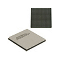
EP4SGX530HH35C2N Altera, EP4SGX530HH35C2N Datasheet - Page 331

EP4SGX530HH35C2N
Manufacturer Part Number
EP4SGX530HH35C2N
Description
IC STRATIX IV FPGA 530K 1152HBGA
Manufacturer
Altera
Series
Stratix® IV GXr
Datasheets
1.EP4SGX110DF29C3N.pdf
(80 pages)
2.EP4SGX110DF29C3N.pdf
(1154 pages)
3.EP4SGX110DF29C3N.pdf
(432 pages)
4.EP4SGX110DF29C3N.pdf
(22 pages)
5.EP4SGX110DF29C3N.pdf
(30 pages)
6.EP4SGX110DF29C3N.pdf
(72 pages)
7.EP4SGX530HH35C2N.pdf
(1145 pages)
Specifications of EP4SGX530HH35C2N
Number Of Logic Elements/cells
531200
Number Of Labs/clbs
21248
Total Ram Bits
27376
Number Of I /o
564
Voltage - Supply
0.87 V ~ 0.93 V
Mounting Type
Surface Mount
Operating Temperature
0°C ~ 85°C
Package / Case
1152-HBGA
Family Name
Stratix® IV
Number Of Logic Blocks/elements
531200
# Registers
424960
# I/os (max)
560
Process Technology
40nm
Operating Supply Voltage (typ)
900mV
Logic Cells
531200
Ram Bits
28033024
Operating Supply Voltage (min)
0.87V
Operating Supply Voltage (max)
0.93V
Operating Temp Range
0C to 85C
Operating Temperature Classification
Commercial
Mounting
Surface Mount
Pin Count
1152
Package Type
FCHBGA
Lead Free Status / RoHS Status
Lead free / RoHS Compliant
Number Of Gates
-
Lead Free Status / Rohs Status
Compliant
Available stocks
Company
Part Number
Manufacturer
Quantity
Price
- EP4SGX110DF29C3N PDF datasheet
- EP4SGX110DF29C3N PDF datasheet #2
- EP4SGX110DF29C3N PDF datasheet #3
- EP4SGX110DF29C3N PDF datasheet #4
- EP4SGX110DF29C3N PDF datasheet #5
- EP4SGX110DF29C3N PDF datasheet #6
- EP4SGX530HH35C2N PDF datasheet #7
- Current page: 331 of 432
- Download datasheet (11Mb)
Chapter 9: Hot Socketing and Power-On Reset in Stratix IV Devices
Hot-Socketing Feature Implementation in Stratix IV Devices
Hot-Socketing Feature Implementation in Stratix IV Devices
Figure 9–1. Hot-Socketing Circuitry for Stratix IV Devices
February 2011 Altera Corporation
1
The hot-socketing feature turns off the output buffer during power up and power
down of the V
circuitry generates an internal HOTSCKT signal when the V
or V
designed to prevent excess I/O leakage during power up. When the voltage ramps up
very slowly, it is still relatively low, even after the POR signal is released and the
configuration is completed. The CONF_DONE, nCEO, and nSTATUS pins fail to respond, as
the output buffer cannot flip from the state set by the hot-socketing circuit at this low
voltage. Therefore, the hot-socketing circuitry has been removed from these
configuration pins to make sure that they are able to operate during configuration.
Thus, it is expected behavior for these pins to drive out during power-up and
power-down sequences.
Figure 9–1
The POR circuit monitors the voltage level of the power supplies (V
V
The weak pull-up resistor (R) in the Stratix IV input/output element (IOE) keeps the
I/O pins from floating. The 3.0-V tolerance control circuit permits the I/O pins to be
driven by 3.0 V before the V
powered. It also prevents the I/O pins from driving out when the device is not in user
mode. To successfully power-up and exit POR on production devices, fully power
V
Altera uses GND as a reference for hot-socketing operations and I/O buffer designs.
To ensure proper operation, you must connect the GND between boards before
connecting the power supplies. This prevents the GND on your board from being
pulled up inadvertently by a path to power through other components on your board.
A pulled up GND could otherwise cause an out-of-specification I/O voltage or
current condition with the Altera device.
CCPGM
CC
Resistor
Pull-Up
Weak
CCPD
before V
PAD
, and V
power supplies are below the threshold voltage. Hot-socketing circuitry is
shows the Stratix IV device’s I/O pin circuitry.
R
CCAUX
CC
CCPD
, V
CCAUX
) and keeps the I/O pins tri-stated until the device is in user mode.
begins to ramp.
V
CCIO
, V
CCIO
CC
, V
, V
CCAUX
Tolerance
to Logic Array
CCPGM
Voltage
Control
Input Buffer
, V
, or V
CCPT
Output Enable
, V
CCPD
CCPGM
power supplies. The hot-socketing
Pre-Driver
Hot Socket
Output
Power On
, or V
Monitor
Reset
CC
Stratix IV Device Handbook Volume 1
, V
CCPD
CCAUX
supplies are
CC
, V
, V
CCIO
CCAUX
, V
CCPGM
, V
CCPT
9–3
,
,
Related parts for EP4SGX530HH35C2N
Image
Part Number
Description
Manufacturer
Datasheet
Request
R

Part Number:
Description:
CYCLONE II STARTER KIT EP2C20N
Manufacturer:
Altera
Datasheet:

Part Number:
Description:
CPLD, EP610 Family, ECMOS Process, 300 Gates, 16 Macro Cells, 16 Reg., 16 User I/Os, 5V Supply, 35 Speed Grade, 24DIP
Manufacturer:
Altera Corporation
Datasheet:

Part Number:
Description:
CPLD, EP610 Family, ECMOS Process, 300 Gates, 16 Macro Cells, 16 Reg., 16 User I/Os, 5V Supply, 15 Speed Grade, 24DIP
Manufacturer:
Altera Corporation
Datasheet:

Part Number:
Description:
Manufacturer:
Altera Corporation
Datasheet:

Part Number:
Description:
CPLD, EP610 Family, ECMOS Process, 300 Gates, 16 Macro Cells, 16 Reg., 16 User I/Os, 5V Supply, 30 Speed Grade, 24DIP
Manufacturer:
Altera Corporation
Datasheet:

Part Number:
Description:
High-performance, low-power erasable programmable logic devices with 8 macrocells, 10ns
Manufacturer:
Altera Corporation
Datasheet:

Part Number:
Description:
High-performance, low-power erasable programmable logic devices with 8 macrocells, 7ns
Manufacturer:
Altera Corporation
Datasheet:

Part Number:
Description:
Classic EPLD
Manufacturer:
Altera Corporation
Datasheet:

Part Number:
Description:
High-performance, low-power erasable programmable logic devices with 8 macrocells, 10ns
Manufacturer:
Altera Corporation
Datasheet:

Part Number:
Description:
Manufacturer:
Altera Corporation
Datasheet:

Part Number:
Description:
Manufacturer:
Altera Corporation
Datasheet:

Part Number:
Description:
Manufacturer:
Altera Corporation
Datasheet:

Part Number:
Description:
CPLD, EP610 Family, ECMOS Process, 300 Gates, 16 Macro Cells, 16 Reg., 16 User I/Os, 5V Supply, 25 Speed Grade, 24DIP
Manufacturer:
Altera Corporation
Datasheet:


