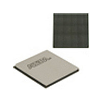
EP4SGX530HH35C2N Altera, EP4SGX530HH35C2N Datasheet - Page 55

EP4SGX530HH35C2N
Manufacturer Part Number
EP4SGX530HH35C2N
Description
IC STRATIX IV FPGA 530K 1152HBGA
Manufacturer
Altera
Series
Stratix® IV GXr
Datasheets
1.EP4SGX110DF29C3N.pdf
(80 pages)
2.EP4SGX110DF29C3N.pdf
(1154 pages)
3.EP4SGX110DF29C3N.pdf
(432 pages)
4.EP4SGX110DF29C3N.pdf
(22 pages)
5.EP4SGX110DF29C3N.pdf
(30 pages)
6.EP4SGX110DF29C3N.pdf
(72 pages)
7.EP4SGX530HH35C2N.pdf
(1145 pages)
Specifications of EP4SGX530HH35C2N
Number Of Logic Elements/cells
531200
Number Of Labs/clbs
21248
Total Ram Bits
27376
Number Of I /o
564
Voltage - Supply
0.87 V ~ 0.93 V
Mounting Type
Surface Mount
Operating Temperature
0°C ~ 85°C
Package / Case
1152-HBGA
Family Name
Stratix® IV
Number Of Logic Blocks/elements
531200
# Registers
424960
# I/os (max)
560
Process Technology
40nm
Operating Supply Voltage (typ)
900mV
Logic Cells
531200
Ram Bits
28033024
Operating Supply Voltage (min)
0.87V
Operating Supply Voltage (max)
0.93V
Operating Temp Range
0C to 85C
Operating Temperature Classification
Commercial
Mounting
Surface Mount
Pin Count
1152
Package Type
FCHBGA
Lead Free Status / RoHS Status
Lead free / RoHS Compliant
Number Of Gates
-
Lead Free Status / Rohs Status
Compliant
Available stocks
Company
Part Number
Manufacturer
Quantity
Price
- EP4SGX110DF29C3N PDF datasheet
- EP4SGX110DF29C3N PDF datasheet #2
- EP4SGX110DF29C3N PDF datasheet #3
- EP4SGX110DF29C3N PDF datasheet #4
- EP4SGX110DF29C3N PDF datasheet #5
- EP4SGX110DF29C3N PDF datasheet #6
- EP4SGX530HH35C2N PDF datasheet #7
- Current page: 55 of 432
- Download datasheet (11Mb)
Chapter 2: Logic Array Blocks and Adaptive Logic Modules in Stratix IV Devices
Document Revision History
Document Revision History
Table 2–1. Document Revision History
February 2011 Altera Corporation
February 2011
November 2009
June 2009
March 2009
November 2008
May 2008
Date
LAB Power Management Techniques
f
Version
The following techniques are used to manage static and dynamic power consumption
within the LAB:
■
■
■
For more information about implementing static and dynamic power consumption
within the LAB, refer to the
Handbook.
Table 2–1
3.0
2.0
3.1
2.2
2.1
1.0
To save AC power, the Quartus II software forces all adder inputs low when ALM
adders are not in use.
Stratix IV LABs operate in high-performance mode or low-power mode. The
Quartus II software automatically chooses the appropriate mode for the LAB,
based on the design, to optimize speed versus leakage trade-offs.
Clocks represent a significant portion of dynamic power consumption due to their
high switching activity and long paths. The LAB clock that distributes a clock
signal to registers within an LAB is a significant contributor to overall clock power
consumption. Each LAB’s clock and clock enable signal are linked. For example, a
combinational ALUT or register in a particular LAB using the labclk1 signal also
uses the labclkena1 signal. To disable LAB-wide clock power consumption
without disabling the entire clock tree, use LAB-wide clock enable to gate the
LAB-wide clock. The Quartus II software automatically promotes register-level
clock enable signals to the LAB-level. All registers within the LAB that share a
common clock and clock enable are controlled by a shared, gated clock. To take
advantage of these clock enables, use a clock-enable construct in your HDL code
for the registered logic.
■
■
■
■
■
■
■
■
Removed “Referenced Documents” section.
■
■
Initial release.
Updated
Applied new template.
Minor text edits.
Updated graphics.
Minor text edits.
Removed the Conclusion section.
Added introductory sentences to improve search ability.
Minor text edits.
Updated Figure 2–6.
Made minor editorial changes.
lists the revision history for this chapter.
Figure
2–6.
Power Optimization
Changes
chapter in volume 2 of the Quartus II
Stratix IV Device Handbook Volume 1
2–19
Related parts for EP4SGX530HH35C2N
Image
Part Number
Description
Manufacturer
Datasheet
Request
R

Part Number:
Description:
CYCLONE II STARTER KIT EP2C20N
Manufacturer:
Altera
Datasheet:

Part Number:
Description:
CPLD, EP610 Family, ECMOS Process, 300 Gates, 16 Macro Cells, 16 Reg., 16 User I/Os, 5V Supply, 35 Speed Grade, 24DIP
Manufacturer:
Altera Corporation
Datasheet:

Part Number:
Description:
CPLD, EP610 Family, ECMOS Process, 300 Gates, 16 Macro Cells, 16 Reg., 16 User I/Os, 5V Supply, 15 Speed Grade, 24DIP
Manufacturer:
Altera Corporation
Datasheet:

Part Number:
Description:
Manufacturer:
Altera Corporation
Datasheet:

Part Number:
Description:
CPLD, EP610 Family, ECMOS Process, 300 Gates, 16 Macro Cells, 16 Reg., 16 User I/Os, 5V Supply, 30 Speed Grade, 24DIP
Manufacturer:
Altera Corporation
Datasheet:

Part Number:
Description:
High-performance, low-power erasable programmable logic devices with 8 macrocells, 10ns
Manufacturer:
Altera Corporation
Datasheet:

Part Number:
Description:
High-performance, low-power erasable programmable logic devices with 8 macrocells, 7ns
Manufacturer:
Altera Corporation
Datasheet:

Part Number:
Description:
Classic EPLD
Manufacturer:
Altera Corporation
Datasheet:

Part Number:
Description:
High-performance, low-power erasable programmable logic devices with 8 macrocells, 10ns
Manufacturer:
Altera Corporation
Datasheet:

Part Number:
Description:
Manufacturer:
Altera Corporation
Datasheet:

Part Number:
Description:
Manufacturer:
Altera Corporation
Datasheet:

Part Number:
Description:
Manufacturer:
Altera Corporation
Datasheet:

Part Number:
Description:
CPLD, EP610 Family, ECMOS Process, 300 Gates, 16 Macro Cells, 16 Reg., 16 User I/Os, 5V Supply, 25 Speed Grade, 24DIP
Manufacturer:
Altera Corporation
Datasheet:


