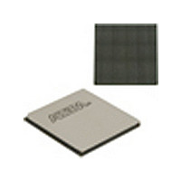
EP4SGX530HH35C2N Altera, EP4SGX530HH35C2N Datasheet - Page 160

EP4SGX530HH35C2N
Manufacturer Part Number
EP4SGX530HH35C2N
Description
IC STRATIX IV FPGA 530K 1152HBGA
Manufacturer
Altera
Series
Stratix® IV GXr
Datasheets
1.EP4SGX110DF29C3N.pdf
(80 pages)
2.EP4SGX110DF29C3N.pdf
(1154 pages)
3.EP4SGX110DF29C3N.pdf
(432 pages)
4.EP4SGX110DF29C3N.pdf
(22 pages)
5.EP4SGX110DF29C3N.pdf
(30 pages)
6.EP4SGX110DF29C3N.pdf
(72 pages)
7.EP4SGX530HH35C2N.pdf
(1145 pages)
Specifications of EP4SGX530HH35C2N
Number Of Logic Elements/cells
531200
Number Of Labs/clbs
21248
Total Ram Bits
27376
Number Of I /o
564
Voltage - Supply
0.87 V ~ 0.93 V
Mounting Type
Surface Mount
Operating Temperature
0°C ~ 85°C
Package / Case
1152-HBGA
Family Name
Stratix® IV
Number Of Logic Blocks/elements
531200
# Registers
424960
# I/os (max)
560
Process Technology
40nm
Operating Supply Voltage (typ)
900mV
Logic Cells
531200
Ram Bits
28033024
Operating Supply Voltage (min)
0.87V
Operating Supply Voltage (max)
0.93V
Operating Temp Range
0C to 85C
Operating Temperature Classification
Commercial
Mounting
Surface Mount
Pin Count
1152
Package Type
FCHBGA
Lead Free Status / RoHS Status
Lead free / RoHS Compliant
Number Of Gates
-
Lead Free Status / Rohs Status
Compliant
Available stocks
Company
Part Number
Manufacturer
Quantity
Price
- EP4SGX110DF29C3N PDF datasheet
- EP4SGX110DF29C3N PDF datasheet #2
- EP4SGX110DF29C3N PDF datasheet #3
- EP4SGX110DF29C3N PDF datasheet #4
- EP4SGX110DF29C3N PDF datasheet #5
- EP4SGX110DF29C3N PDF datasheet #6
- EP4SGX530HH35C2N PDF datasheet #7
- Current page: 160 of 432
- Download datasheet (11Mb)
5–44
Figure 5–39. PLL Reconfiguration Scan Chain
Notes to
(1) Stratix IV left and right PLLs support
(2) i = 6 or i = 9.
(3) This figure shows the corresponding scan register for the K counter in between the scan registers for the charge pump and loop filter. The K
Stratix IV Device Handbook Volume 1
scanclkena
configupdate
scandataout
counter is physically located after the VCO.
scandone
scandata
Figure
inclk
scanclk
5–39:
1
PLL Reconfiguration Hardware Implementation
The following PLL components are reconfigurable in real time:
■
■
■
■
■
Figure 5–39
shifting their new settings into a serial shift-register chain or scan chain. Serial data is
input to the scan chain using the scandata port. Shift registers are clocked by scanclk.
The maximum scanclk frequency is 100 MHz. Serial data is shifted through the scan
chain as long as the scanclkena signal stays asserted. After the last bit of data is
clocked, asserting the configupdate signal for at least one scanclk clock cycle causes
the PLL configuration bits to be synchronously updated with the data in the scan
registers.
The counter settings are updated synchronously to the clock frequency of the
individual counters. Therefore, all counters are not updated simultaneously.
from m counter
from n counter
/Ci (2)
Pre-scale counter (n)
Feedback counter (m)
Post-scale output counters (C0 - C9)
Post VCO Divider (K)
Dynamically adjust the charge-pump current (Icp) and loop-filter components
(R, C) to facilitate reconfiguration of the PLL bandwidth
C0 - C6
/Ci-1
shows how you can dynamically adjust the PLL counter settings by
counters.
(Note 1)
PFD
/C2
LF/K/CP (3)
/C1
Chapter 5: Clock Networks and PLLs in Stratix IV Devices
/C0
VCO
February 2011 Altera Corporation
/m
PLLs in Stratix IV Devices
/n
Related parts for EP4SGX530HH35C2N
Image
Part Number
Description
Manufacturer
Datasheet
Request
R

Part Number:
Description:
CYCLONE II STARTER KIT EP2C20N
Manufacturer:
Altera
Datasheet:

Part Number:
Description:
CPLD, EP610 Family, ECMOS Process, 300 Gates, 16 Macro Cells, 16 Reg., 16 User I/Os, 5V Supply, 35 Speed Grade, 24DIP
Manufacturer:
Altera Corporation
Datasheet:

Part Number:
Description:
CPLD, EP610 Family, ECMOS Process, 300 Gates, 16 Macro Cells, 16 Reg., 16 User I/Os, 5V Supply, 15 Speed Grade, 24DIP
Manufacturer:
Altera Corporation
Datasheet:

Part Number:
Description:
Manufacturer:
Altera Corporation
Datasheet:

Part Number:
Description:
CPLD, EP610 Family, ECMOS Process, 300 Gates, 16 Macro Cells, 16 Reg., 16 User I/Os, 5V Supply, 30 Speed Grade, 24DIP
Manufacturer:
Altera Corporation
Datasheet:

Part Number:
Description:
High-performance, low-power erasable programmable logic devices with 8 macrocells, 10ns
Manufacturer:
Altera Corporation
Datasheet:

Part Number:
Description:
High-performance, low-power erasable programmable logic devices with 8 macrocells, 7ns
Manufacturer:
Altera Corporation
Datasheet:

Part Number:
Description:
Classic EPLD
Manufacturer:
Altera Corporation
Datasheet:

Part Number:
Description:
High-performance, low-power erasable programmable logic devices with 8 macrocells, 10ns
Manufacturer:
Altera Corporation
Datasheet:

Part Number:
Description:
Manufacturer:
Altera Corporation
Datasheet:

Part Number:
Description:
Manufacturer:
Altera Corporation
Datasheet:

Part Number:
Description:
Manufacturer:
Altera Corporation
Datasheet:

Part Number:
Description:
CPLD, EP610 Family, ECMOS Process, 300 Gates, 16 Macro Cells, 16 Reg., 16 User I/Os, 5V Supply, 25 Speed Grade, 24DIP
Manufacturer:
Altera Corporation
Datasheet:


