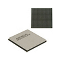
EP4SGX530HH35C2N Altera, EP4SGX530HH35C2N Datasheet - Page 287

EP4SGX530HH35C2N
Manufacturer Part Number
EP4SGX530HH35C2N
Description
IC STRATIX IV FPGA 530K 1152HBGA
Manufacturer
Altera
Series
Stratix® IV GXr
Datasheets
1.EP4SGX110DF29C3N.pdf
(80 pages)
2.EP4SGX110DF29C3N.pdf
(1154 pages)
3.EP4SGX110DF29C3N.pdf
(432 pages)
4.EP4SGX110DF29C3N.pdf
(22 pages)
5.EP4SGX110DF29C3N.pdf
(30 pages)
6.EP4SGX110DF29C3N.pdf
(72 pages)
7.EP4SGX530HH35C2N.pdf
(1145 pages)
Specifications of EP4SGX530HH35C2N
Number Of Logic Elements/cells
531200
Number Of Labs/clbs
21248
Total Ram Bits
27376
Number Of I /o
564
Voltage - Supply
0.87 V ~ 0.93 V
Mounting Type
Surface Mount
Operating Temperature
0°C ~ 85°C
Package / Case
1152-HBGA
Family Name
Stratix® IV
Number Of Logic Blocks/elements
531200
# Registers
424960
# I/os (max)
560
Process Technology
40nm
Operating Supply Voltage (typ)
900mV
Logic Cells
531200
Ram Bits
28033024
Operating Supply Voltage (min)
0.87V
Operating Supply Voltage (max)
0.93V
Operating Temp Range
0C to 85C
Operating Temperature Classification
Commercial
Mounting
Surface Mount
Pin Count
1152
Package Type
FCHBGA
Lead Free Status / RoHS Status
Lead free / RoHS Compliant
Number Of Gates
-
Lead Free Status / Rohs Status
Compliant
Available stocks
Company
Part Number
Manufacturer
Quantity
Price
- EP4SGX110DF29C3N PDF datasheet
- EP4SGX110DF29C3N PDF datasheet #2
- EP4SGX110DF29C3N PDF datasheet #3
- EP4SGX110DF29C3N PDF datasheet #4
- EP4SGX110DF29C3N PDF datasheet #5
- EP4SGX110DF29C3N PDF datasheet #6
- EP4SGX530HH35C2N PDF datasheet #7
- Current page: 287 of 432
- Download datasheet (11Mb)
Chapter 8: High-Speed Differential I/O Interfaces and DPA in Stratix IV Devices
ALTLVDS Port List
ALTLVDS Port List
Table 8–7. Port List of the LVDS Interface (ALTLVDS)
February 2011 Altera Corporation
PLL Signals
pll_areset
LVDS Transmitter Interface Signals
tx_in[ ]
tx_inclock
tx_enable
tx_out
tx_outclock
tx_coreclock
tx_locked
Port Name
(3)
(3)
Table 8–7
lists the interface signals for an LVDS transmitter and receiver.
Input
Input
Input
Input
Output
Output
Output
Output
Output
Input /
Asynchronous reset to the LVDS transmitter and receiver PLL. The
minimum pulse width requirement for this signal is 10 ns.
The data bus width per channel is the same as the serialization factor (SF).
Input data must be synchronous to the tx_coreclock signal.
Reference clock input for the transmitter PLL.
The ALTLVDS MegaWizard Plug-In Manager software automatically selects
the appropriate PLL multiplication factor based on the data rate and
reference clock frequency selection.
For more information about the allowed frequency range for this reference
clock, refer to the “High-Speed I/O Specification” section in the
Switching Characteristics for Stratix IV Devices
This port is instantiated only when you select the Use External PLL option
in the MegaWizard Plug-In Manager software. This input port must be
driven by the PLL instantiated though the ALTPLL MegaWizard Plug-In
Manager software.
LVDS transmitter serial data output port. tx_out is clocked by a serial clock
generated by the left and right PLL.
The frequency of this clock is programmable to be the same as the data
rate, half the data rate, or one-fourth the data rate. The phase offset of this
clock, with respect to the serial data, is programmable in increments of 45°.
FPGA fabric-transmitter interface clock. The parallel transmitter data
generated in the FPGA fabric must be clocked with this clock.
This port is not available when you select the Use External PLL option in the
MegaWizard Plug-In Manager software. The FPGA fabric-transmitter
interface clock must be driven by the PLL instantiated through the ALTPLL
MegaWizard Plug-In Manager software.
When high, this signal indicates that the transmitter PLL is locked to the
input reference clock.
(Note
1),
(2)
(Part 1 of 3)
Description
Stratix IV Device Handbook Volume 1
chapter.
DC and
8–9
Related parts for EP4SGX530HH35C2N
Image
Part Number
Description
Manufacturer
Datasheet
Request
R

Part Number:
Description:
CYCLONE II STARTER KIT EP2C20N
Manufacturer:
Altera
Datasheet:

Part Number:
Description:
CPLD, EP610 Family, ECMOS Process, 300 Gates, 16 Macro Cells, 16 Reg., 16 User I/Os, 5V Supply, 35 Speed Grade, 24DIP
Manufacturer:
Altera Corporation
Datasheet:

Part Number:
Description:
CPLD, EP610 Family, ECMOS Process, 300 Gates, 16 Macro Cells, 16 Reg., 16 User I/Os, 5V Supply, 15 Speed Grade, 24DIP
Manufacturer:
Altera Corporation
Datasheet:

Part Number:
Description:
Manufacturer:
Altera Corporation
Datasheet:

Part Number:
Description:
CPLD, EP610 Family, ECMOS Process, 300 Gates, 16 Macro Cells, 16 Reg., 16 User I/Os, 5V Supply, 30 Speed Grade, 24DIP
Manufacturer:
Altera Corporation
Datasheet:

Part Number:
Description:
High-performance, low-power erasable programmable logic devices with 8 macrocells, 10ns
Manufacturer:
Altera Corporation
Datasheet:

Part Number:
Description:
High-performance, low-power erasable programmable logic devices with 8 macrocells, 7ns
Manufacturer:
Altera Corporation
Datasheet:

Part Number:
Description:
Classic EPLD
Manufacturer:
Altera Corporation
Datasheet:

Part Number:
Description:
High-performance, low-power erasable programmable logic devices with 8 macrocells, 10ns
Manufacturer:
Altera Corporation
Datasheet:

Part Number:
Description:
Manufacturer:
Altera Corporation
Datasheet:

Part Number:
Description:
Manufacturer:
Altera Corporation
Datasheet:

Part Number:
Description:
Manufacturer:
Altera Corporation
Datasheet:

Part Number:
Description:
CPLD, EP610 Family, ECMOS Process, 300 Gates, 16 Macro Cells, 16 Reg., 16 User I/Os, 5V Supply, 25 Speed Grade, 24DIP
Manufacturer:
Altera Corporation
Datasheet:


