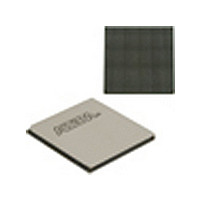
EP4SGX530HH35C2N Altera, EP4SGX530HH35C2N Datasheet - Page 356

EP4SGX530HH35C2N
Manufacturer Part Number
EP4SGX530HH35C2N
Description
IC STRATIX IV FPGA 530K 1152HBGA
Manufacturer
Altera
Series
Stratix® IV GXr
Datasheets
1.EP4SGX110DF29C3N.pdf
(80 pages)
2.EP4SGX110DF29C3N.pdf
(1154 pages)
3.EP4SGX110DF29C3N.pdf
(432 pages)
4.EP4SGX110DF29C3N.pdf
(22 pages)
5.EP4SGX110DF29C3N.pdf
(30 pages)
6.EP4SGX110DF29C3N.pdf
(72 pages)
7.EP4SGX530HH35C2N.pdf
(1145 pages)
Specifications of EP4SGX530HH35C2N
Number Of Logic Elements/cells
531200
Number Of Labs/clbs
21248
Total Ram Bits
27376
Number Of I /o
564
Voltage - Supply
0.87 V ~ 0.93 V
Mounting Type
Surface Mount
Operating Temperature
0°C ~ 85°C
Package / Case
1152-HBGA
Family Name
Stratix® IV
Number Of Logic Blocks/elements
531200
# Registers
424960
# I/os (max)
560
Process Technology
40nm
Operating Supply Voltage (typ)
900mV
Logic Cells
531200
Ram Bits
28033024
Operating Supply Voltage (min)
0.87V
Operating Supply Voltage (max)
0.93V
Operating Temp Range
0C to 85C
Operating Temperature Classification
Commercial
Mounting
Surface Mount
Pin Count
1152
Package Type
FCHBGA
Lead Free Status / RoHS Status
Lead free / RoHS Compliant
Number Of Gates
-
Lead Free Status / Rohs Status
Compliant
Available stocks
Company
Part Number
Manufacturer
Quantity
Price
- EP4SGX110DF29C3N PDF datasheet
- EP4SGX110DF29C3N PDF datasheet #2
- EP4SGX110DF29C3N PDF datasheet #3
- EP4SGX110DF29C3N PDF datasheet #4
- EP4SGX110DF29C3N PDF datasheet #5
- EP4SGX110DF29C3N PDF datasheet #6
- EP4SGX530HH35C2N PDF datasheet #7
- Current page: 356 of 432
- Download datasheet (11Mb)
10–22
Figure 10–8. Multi-Device Fast AS Configuration When the Devices Receive the Same Data Using a Single .sof
Notes to
(1) Connect the pull-up resistors to V
(2) Connect the repeater buffers between the Stratix IV master and slave device(s) for DATA[0] and DCLK. This is to prevent potential signal
Stratix IV Device Handbook Volume 1
integrity and clock skew problems.
Figure
Estimating Active Serial Configuration Time
10–8:
1
Serial Configuration
Figure 10–8
the same data using a single .sof.
Active serial configuration time is dominated by the time it takes to transfer data from
the serial configuration device to the Stratix IV device. This serial interface is clocked
by the Stratix IV DCLK output (generated from an internal oscillator) and must be set to
40 MHz (25 ns).Therefore, the minimum configuration time estimate for an EP4SE230
device (94, 600, 000 bits of uncompressed data) is:
RBF Size × (minimum DCLK period / 1 bit per DCLK cycle) = estimated minimum
configuration time
94, 600, 000 bits × (25 ns / 1 bit) = 2365 ms
The calculation above is based on a preliminary uncompressed .rbf size. The final .rbf
size will be available after the Quartus II software is able to generate the .rbf.
Enabling compression reduces the amount of configuration data that is transmitted to
the Stratix IV device, which also reduces configuration time. On average, compression
reduces configuration time, depending on the design.
Device
DATA
DCLK
ASDI
nCS
V
CCPGM (1)
CCPGM
10 kΩ
at a 3.0-V supply.
V
shows the multi-device fast AS configuration when the devices receive
CCPGM (1)
Buffers (2)
Chapter 10: Configuration, Design Security, and Remote System Upgrades in Stratix IV Devices
10 kΩ
V
GND
CCPGM (1)
10 kΩ
nSTATUS
CONF_DONE
nCONFIG
nCE
DATA0
DCLK
nCSO
ASDO
Device Master
Stratix IV
MSEL2
MSEL1
MSEL0
nCEO
V
N.C.
CCPGM
GND
GND
Fast Active Serial Configuration (Serial Configuration Devices)
nSTATUS
CONF_DONE
nCONFIG
nCE
DATA0
DCLK
nSTATUS
CONF_DONE
nCONFIG
nCE
DATA0
DCLK
nSTATUS
CONF_DONE
nCONFIG
nCE
DATA0
DCLK
Device Slave
Device Slave
Device Slave
Stratix IV
Stratix IV
Stratix IV
MSEL2
MSEL1
MSEL0
MSEL2
MSEL1
MSEL0
MSEL2
MSEL1
MSEL0
nCEO
nCEO
nCEO
April 2011 Altera Corporation
GND
GND
GND
N.C.
N.C.
N.C.
V
V
V
CCPGM
CCPGM
CCPGM
Related parts for EP4SGX530HH35C2N
Image
Part Number
Description
Manufacturer
Datasheet
Request
R

Part Number:
Description:
CYCLONE II STARTER KIT EP2C20N
Manufacturer:
Altera
Datasheet:

Part Number:
Description:
CPLD, EP610 Family, ECMOS Process, 300 Gates, 16 Macro Cells, 16 Reg., 16 User I/Os, 5V Supply, 35 Speed Grade, 24DIP
Manufacturer:
Altera Corporation
Datasheet:

Part Number:
Description:
CPLD, EP610 Family, ECMOS Process, 300 Gates, 16 Macro Cells, 16 Reg., 16 User I/Os, 5V Supply, 15 Speed Grade, 24DIP
Manufacturer:
Altera Corporation
Datasheet:

Part Number:
Description:
Manufacturer:
Altera Corporation
Datasheet:

Part Number:
Description:
CPLD, EP610 Family, ECMOS Process, 300 Gates, 16 Macro Cells, 16 Reg., 16 User I/Os, 5V Supply, 30 Speed Grade, 24DIP
Manufacturer:
Altera Corporation
Datasheet:

Part Number:
Description:
High-performance, low-power erasable programmable logic devices with 8 macrocells, 10ns
Manufacturer:
Altera Corporation
Datasheet:

Part Number:
Description:
High-performance, low-power erasable programmable logic devices with 8 macrocells, 7ns
Manufacturer:
Altera Corporation
Datasheet:

Part Number:
Description:
Classic EPLD
Manufacturer:
Altera Corporation
Datasheet:

Part Number:
Description:
High-performance, low-power erasable programmable logic devices with 8 macrocells, 10ns
Manufacturer:
Altera Corporation
Datasheet:

Part Number:
Description:
Manufacturer:
Altera Corporation
Datasheet:

Part Number:
Description:
Manufacturer:
Altera Corporation
Datasheet:

Part Number:
Description:
Manufacturer:
Altera Corporation
Datasheet:

Part Number:
Description:
CPLD, EP610 Family, ECMOS Process, 300 Gates, 16 Macro Cells, 16 Reg., 16 User I/Os, 5V Supply, 25 Speed Grade, 24DIP
Manufacturer:
Altera Corporation
Datasheet:


