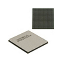
EP4SGX530HH35C2N Altera, EP4SGX530HH35C2N Datasheet - Page 368

EP4SGX530HH35C2N
Manufacturer Part Number
EP4SGX530HH35C2N
Description
IC STRATIX IV FPGA 530K 1152HBGA
Manufacturer
Altera
Series
Stratix® IV GXr
Datasheets
1.EP4SGX110DF29C3N.pdf
(80 pages)
2.EP4SGX110DF29C3N.pdf
(1154 pages)
3.EP4SGX110DF29C3N.pdf
(432 pages)
4.EP4SGX110DF29C3N.pdf
(22 pages)
5.EP4SGX110DF29C3N.pdf
(30 pages)
6.EP4SGX110DF29C3N.pdf
(72 pages)
7.EP4SGX530HH35C2N.pdf
(1145 pages)
Specifications of EP4SGX530HH35C2N
Number Of Logic Elements/cells
531200
Number Of Labs/clbs
21248
Total Ram Bits
27376
Number Of I /o
564
Voltage - Supply
0.87 V ~ 0.93 V
Mounting Type
Surface Mount
Operating Temperature
0°C ~ 85°C
Package / Case
1152-HBGA
Family Name
Stratix® IV
Number Of Logic Blocks/elements
531200
# Registers
424960
# I/os (max)
560
Process Technology
40nm
Operating Supply Voltage (typ)
900mV
Logic Cells
531200
Ram Bits
28033024
Operating Supply Voltage (min)
0.87V
Operating Supply Voltage (max)
0.93V
Operating Temp Range
0C to 85C
Operating Temperature Classification
Commercial
Mounting
Surface Mount
Pin Count
1152
Package Type
FCHBGA
Lead Free Status / RoHS Status
Lead free / RoHS Compliant
Number Of Gates
-
Lead Free Status / Rohs Status
Compliant
Available stocks
Company
Part Number
Manufacturer
Quantity
Price
- EP4SGX110DF29C3N PDF datasheet
- EP4SGX110DF29C3N PDF datasheet #2
- EP4SGX110DF29C3N PDF datasheet #3
- EP4SGX110DF29C3N PDF datasheet #4
- EP4SGX110DF29C3N PDF datasheet #5
- EP4SGX110DF29C3N PDF datasheet #6
- EP4SGX530HH35C2N PDF datasheet #7
- Current page: 368 of 432
- Download datasheet (11Mb)
10–34
Figure 10–15. Multi-Device PS Configuration Using a USB Blaster, EthernetBlaster, MasterBlaster, ByteBlaster II, or
ByteBlasterMV Cable
Notes to
(1) Connect the pull-up resistor to the same supply voltage (V
(2) You only need the pull-up resistors on DATA0 and DCLK if the download cable is the only configuration scheme used on your board. This is to
(3) Pin 6 of the header is a V
Stratix IV Device Handbook Volume 1
EthernetBlaster cable.
ensure that DATA0 and DCLK are not left floating after configuration. For example, if you are also using a configuration device, you do not need
the pull-up resistors on DATA0 and DCLK.
this value, refer to the
this pin is a no connect.
Figure
10–15:
10 kΩ
V
CCPGM
10 kΩ
V
MasterBlaster Serial/USB Communications Cable User
CCPGM
(1)
You can use a download cable to configure multiple Stratix IV devices by connecting
each device’s nCEO pin to the subsequent device’s nCE pin. The first device’s nCE pin is
connected to GND, while its nCEO pin is connected to the nCE of the next device in the
chain. The last device’s nCE input comes from the previous device, while its nCEO pin is
left floating. All other configuration pins (nCONFIG, nSTATUS, DCLK, DATA0, and
CONF_DONE) are connected to every device in the chain. Because all CONF_DONE pins are
tied together, all devices in the chain initialize and enter user mode at the same time.
In addition, because the nSTATUS pins are tied together, the entire chain halts
configuration if any device detects an error. The Auto-restart configuration after
error option does not affect the configuration cycle because you must manually restart
the configuration in the Quartus II software when an error occurs.
Figure 10–15
cable.
IO
reference voltage for the MasterBlaster output driver. V
(2)
(1)
V
V
CCPGM
CCPGM
GND
GND
GND
(1)
(1)
shows how to configure multiple Stratix IV devices with a download
Chapter 10: Configuration, Design Security, and Remote System Upgrades in Stratix IV Devices
MSEL2
MSEL1
MSEL0
Stratix IV Device 1
MSEL2
MSEL1
MSEL0
DATA0
nCONFIG
nCONFIG
nCE
Stratix IV Device 2
nCE
DATA0
CONF_DONE
CONF_DONE
nSTATUS
nSTATUS
CCPGM
DCLK
nCEO
nCEO
DCLK
) as the USB Blaster, MasterBlaster (VIO pin), ByteBlaster II, ByteBlasterMV, or
10 kΩ
V
N.C.
CCPGM
10 kΩ
Guide. In the USB-Blaster, ByteBlaster II, and ByteBlasterMV cables,
V
(1)
CCPGM
IO
must match the device’s V
(1)
10 kΩ
V
CCPGM
(2)
(1)
10-Pin Male Header
Pin 1
Download Cable
(PS Mode)
CCPGM
GND
April 2011 Altera Corporation
V
CCPGM
. For more information about
Passive Serial Configuration
V
GND
IO
(1)
(3)
Related parts for EP4SGX530HH35C2N
Image
Part Number
Description
Manufacturer
Datasheet
Request
R

Part Number:
Description:
CYCLONE II STARTER KIT EP2C20N
Manufacturer:
Altera
Datasheet:

Part Number:
Description:
CPLD, EP610 Family, ECMOS Process, 300 Gates, 16 Macro Cells, 16 Reg., 16 User I/Os, 5V Supply, 35 Speed Grade, 24DIP
Manufacturer:
Altera Corporation
Datasheet:

Part Number:
Description:
CPLD, EP610 Family, ECMOS Process, 300 Gates, 16 Macro Cells, 16 Reg., 16 User I/Os, 5V Supply, 15 Speed Grade, 24DIP
Manufacturer:
Altera Corporation
Datasheet:

Part Number:
Description:
Manufacturer:
Altera Corporation
Datasheet:

Part Number:
Description:
CPLD, EP610 Family, ECMOS Process, 300 Gates, 16 Macro Cells, 16 Reg., 16 User I/Os, 5V Supply, 30 Speed Grade, 24DIP
Manufacturer:
Altera Corporation
Datasheet:

Part Number:
Description:
High-performance, low-power erasable programmable logic devices with 8 macrocells, 10ns
Manufacturer:
Altera Corporation
Datasheet:

Part Number:
Description:
High-performance, low-power erasable programmable logic devices with 8 macrocells, 7ns
Manufacturer:
Altera Corporation
Datasheet:

Part Number:
Description:
Classic EPLD
Manufacturer:
Altera Corporation
Datasheet:

Part Number:
Description:
High-performance, low-power erasable programmable logic devices with 8 macrocells, 10ns
Manufacturer:
Altera Corporation
Datasheet:

Part Number:
Description:
Manufacturer:
Altera Corporation
Datasheet:

Part Number:
Description:
Manufacturer:
Altera Corporation
Datasheet:

Part Number:
Description:
Manufacturer:
Altera Corporation
Datasheet:

Part Number:
Description:
CPLD, EP610 Family, ECMOS Process, 300 Gates, 16 Macro Cells, 16 Reg., 16 User I/Os, 5V Supply, 25 Speed Grade, 24DIP
Manufacturer:
Altera Corporation
Datasheet:


