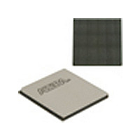
EP4SGX530HH35C2N Altera, EP4SGX530HH35C2N Datasheet - Page 177

EP4SGX530HH35C2N
Manufacturer Part Number
EP4SGX530HH35C2N
Description
IC STRATIX IV FPGA 530K 1152HBGA
Manufacturer
Altera
Series
Stratix® IV GXr
Datasheets
1.EP4SGX110DF29C3N.pdf
(80 pages)
2.EP4SGX110DF29C3N.pdf
(1154 pages)
3.EP4SGX110DF29C3N.pdf
(432 pages)
4.EP4SGX110DF29C3N.pdf
(22 pages)
5.EP4SGX110DF29C3N.pdf
(30 pages)
6.EP4SGX110DF29C3N.pdf
(72 pages)
7.EP4SGX530HH35C2N.pdf
(1145 pages)
Specifications of EP4SGX530HH35C2N
Number Of Logic Elements/cells
531200
Number Of Labs/clbs
21248
Total Ram Bits
27376
Number Of I /o
564
Voltage - Supply
0.87 V ~ 0.93 V
Mounting Type
Surface Mount
Operating Temperature
0°C ~ 85°C
Package / Case
1152-HBGA
Family Name
Stratix® IV
Number Of Logic Blocks/elements
531200
# Registers
424960
# I/os (max)
560
Process Technology
40nm
Operating Supply Voltage (typ)
900mV
Logic Cells
531200
Ram Bits
28033024
Operating Supply Voltage (min)
0.87V
Operating Supply Voltage (max)
0.93V
Operating Temp Range
0C to 85C
Operating Temperature Classification
Commercial
Mounting
Surface Mount
Pin Count
1152
Package Type
FCHBGA
Lead Free Status / RoHS Status
Lead free / RoHS Compliant
Number Of Gates
-
Lead Free Status / Rohs Status
Compliant
Available stocks
Company
Part Number
Manufacturer
Quantity
Price
- EP4SGX110DF29C3N PDF datasheet
- EP4SGX110DF29C3N PDF datasheet #2
- EP4SGX110DF29C3N PDF datasheet #3
- EP4SGX110DF29C3N PDF datasheet #4
- EP4SGX110DF29C3N PDF datasheet #5
- EP4SGX110DF29C3N PDF datasheet #6
- EP4SGX530HH35C2N PDF datasheet #7
- Current page: 177 of 432
- Download datasheet (11Mb)
Chapter 6: I/O Features in Stratix IV Devices
I/O Banks
Table 6–2. I/O Standards and Voltage Levels for Stratix IV Devices
I/O Banks
February 2011 Altera Corporation
LVPECL
Notes to
(1) V
(2) Single-ended HSTL/SSTL, differential SSTL/HSTL, and LVDS input buffers are powered by V
(3) For more information about the 3.3-V LVTTL/LVCMOS standard supported in Stratix IV devices, refer to
(4) Column I/O banks support LVPECL I/O standards for input clock operation. Clock inputs on column I/Os are powered by V
(5) Column and row I/O banks support LVDS outputs using two single-ended output buffers, an external one-resistor (LVDS_E_1R), and a
(6) Row I/O banks support RSDS and mini-LVDS I/O standards using a true LVDS output buffer without a resistor network.
(7) Column and row I/O banks support RSDS and mini-LVDS I/O standards using two single-ended output buffers with one-resistor (RSDS_E_1R
(8) The emulated differential output standard that supports the tri-state feature includes: LVDS_E_1R, LVDS_E_3R, RSDS_E_1R, RSDS_E_3R,
I/O Standard
input buffers and true differential output buffers. Column I/O banks support true differential input buffers, but not true differential output buffers.
I/O pins are organized in pairs to support differential standards. Column I/O differential HSTL and SSTL inputs use LVDS differential input buffers
without on-chip R
as differential clock inputs. They are powered by V
powered by V
three-resistor (LVDS_E_3R) network.
and mini-LVDS_E_1R) and three-resistor (RSDS_E_3R and mini-LVDS_E_3R) networks.
Mini_LVDS_E_1R, and Mini_LVDS_E_3R. For more information, refer to the
CCPD
Table
is either 2.5 or 3.0 V. For V
6–2:
f
f
CCPD
.
D
support.
For more information about electrical characteristics of each I/O standard, refer to the
DC and Switching Characteristics for Stratix IV Devices
Stratix IV devices contain up to 24 I/O banks, as shown in
The row I/O banks contain true differential input and output buffers and dedicated
circuitry to support differential standards at speeds up to 1.6 Gbps.
Each I/O bank in Stratix IV devices can support high-performance external memory
interfaces with dedicated circuitry. The I/O pins are organized in pairs to support
differential standards. Each I/O pin pair can support both differential input and
output buffers. The only exceptions are the clk[1,3,8,10], PLL_L[1,4]_clk, and
PLL_R[1,4]_clk pins, which support differential input operations only.
For the number of channels available for the LVDS I/O standard, refer to the
High-Speed Differential I/O Interface and DPA in Stratix IV Devices
information about transceiver-bank-related features, refer to the
Architecture in Stratix IV Devices
Standard
Support
—
CCIO
= 3.0 V, V
I/O Banks
Column
Input Operation
(4)
CCPD
CCIO
= 3.0 V. For V
I/O Banks
when configured as single-ended clock inputs. Differential clock inputs in row I/Os are
Row
2.5
V
CCIO
CCIO
chapter.
(V)
I/O Banks
Column
= 2.5 V or less, V
Output Operation
—
I/O Buffer (ALTIOBUF) Megafunction User
(Note 1)
I/O Banks
Row
CCPD
—
(Part 3 of 3)
= 2.5 V.
CCPD
. Row I/O banks support both true differential
chapter.
(Pre-Driver
V
Voltage)
CCPD
2.5
“3.3-V I/O Interface” on page
Figure 6–1
Stratix IV Device Handbook Volume 1
(V)
chapter. For more
Transceiver
(Input Ref
Voltage)
V
REF
—
CCCLKIN
Guide.
and
(V)
when configured
Figure
Termination
Voltage)
(Board
V
TT
6–19.
—
(V)
6–2.
6–5
Related parts for EP4SGX530HH35C2N
Image
Part Number
Description
Manufacturer
Datasheet
Request
R

Part Number:
Description:
CYCLONE II STARTER KIT EP2C20N
Manufacturer:
Altera
Datasheet:

Part Number:
Description:
CPLD, EP610 Family, ECMOS Process, 300 Gates, 16 Macro Cells, 16 Reg., 16 User I/Os, 5V Supply, 35 Speed Grade, 24DIP
Manufacturer:
Altera Corporation
Datasheet:

Part Number:
Description:
CPLD, EP610 Family, ECMOS Process, 300 Gates, 16 Macro Cells, 16 Reg., 16 User I/Os, 5V Supply, 15 Speed Grade, 24DIP
Manufacturer:
Altera Corporation
Datasheet:

Part Number:
Description:
Manufacturer:
Altera Corporation
Datasheet:

Part Number:
Description:
CPLD, EP610 Family, ECMOS Process, 300 Gates, 16 Macro Cells, 16 Reg., 16 User I/Os, 5V Supply, 30 Speed Grade, 24DIP
Manufacturer:
Altera Corporation
Datasheet:

Part Number:
Description:
High-performance, low-power erasable programmable logic devices with 8 macrocells, 10ns
Manufacturer:
Altera Corporation
Datasheet:

Part Number:
Description:
High-performance, low-power erasable programmable logic devices with 8 macrocells, 7ns
Manufacturer:
Altera Corporation
Datasheet:

Part Number:
Description:
Classic EPLD
Manufacturer:
Altera Corporation
Datasheet:

Part Number:
Description:
High-performance, low-power erasable programmable logic devices with 8 macrocells, 10ns
Manufacturer:
Altera Corporation
Datasheet:

Part Number:
Description:
Manufacturer:
Altera Corporation
Datasheet:

Part Number:
Description:
Manufacturer:
Altera Corporation
Datasheet:

Part Number:
Description:
Manufacturer:
Altera Corporation
Datasheet:

Part Number:
Description:
CPLD, EP610 Family, ECMOS Process, 300 Gates, 16 Macro Cells, 16 Reg., 16 User I/Os, 5V Supply, 25 Speed Grade, 24DIP
Manufacturer:
Altera Corporation
Datasheet:


