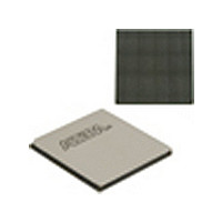
EP4SGX530HH35C2N Altera, EP4SGX530HH35C2N Datasheet - Page 347

EP4SGX530HH35C2N
Manufacturer Part Number
EP4SGX530HH35C2N
Description
IC STRATIX IV FPGA 530K 1152HBGA
Manufacturer
Altera
Series
Stratix® IV GXr
Datasheets
1.EP4SGX110DF29C3N.pdf
(80 pages)
2.EP4SGX110DF29C3N.pdf
(1154 pages)
3.EP4SGX110DF29C3N.pdf
(432 pages)
4.EP4SGX110DF29C3N.pdf
(22 pages)
5.EP4SGX110DF29C3N.pdf
(30 pages)
6.EP4SGX110DF29C3N.pdf
(72 pages)
7.EP4SGX530HH35C2N.pdf
(1145 pages)
Specifications of EP4SGX530HH35C2N
Number Of Logic Elements/cells
531200
Number Of Labs/clbs
21248
Total Ram Bits
27376
Number Of I /o
564
Voltage - Supply
0.87 V ~ 0.93 V
Mounting Type
Surface Mount
Operating Temperature
0°C ~ 85°C
Package / Case
1152-HBGA
Family Name
Stratix® IV
Number Of Logic Blocks/elements
531200
# Registers
424960
# I/os (max)
560
Process Technology
40nm
Operating Supply Voltage (typ)
900mV
Logic Cells
531200
Ram Bits
28033024
Operating Supply Voltage (min)
0.87V
Operating Supply Voltage (max)
0.93V
Operating Temp Range
0C to 85C
Operating Temperature Classification
Commercial
Mounting
Surface Mount
Pin Count
1152
Package Type
FCHBGA
Lead Free Status / RoHS Status
Lead free / RoHS Compliant
Number Of Gates
-
Lead Free Status / Rohs Status
Compliant
Available stocks
Company
Part Number
Manufacturer
Quantity
Price
- EP4SGX110DF29C3N PDF datasheet
- EP4SGX110DF29C3N PDF datasheet #2
- EP4SGX110DF29C3N PDF datasheet #3
- EP4SGX110DF29C3N PDF datasheet #4
- EP4SGX110DF29C3N PDF datasheet #5
- EP4SGX110DF29C3N PDF datasheet #6
- EP4SGX530HH35C2N PDF datasheet #7
- Current page: 347 of 432
- Download datasheet (11Mb)
Chapter 10: Configuration, Design Security, and Remote System Upgrades in Stratix IV Devices
Fast Passive Parallel Configuration
Table 10–4. FPP Timing Parameters for Stratix IV Devices (Part 2 of 2)
April 2011 Altera Corporation
t
t
t
T
t
t
t
t
t
t
t
f
Notes to
(1) This information is preliminary.
(2) Use these timing parameters when you have not enabled the decompression and design security features.
(3) You can obtain this value if you do not delay the configuration by extending the nCONFIG or nSTATUS low pulse width.
(4) This value is applicable if you do not delay the configuration by externally holding nSTATUS low.
(5) The minimum and maximum numbers apply only if you chose the internal oscillator as the clock source for starting the device.
(6) Adding up t
(7) Applicable to EP4SE230, EP4SE360, EP4SGX70, EP4SGX110, EP4SGX180, EP4SGX230, EP4SGX290 (except F45 package), EP4SGX360 (except
(8) Applicable to EP4SE530, EP4SGX290 (only for F45 package), EP4SGX360 (only for F45 package), EP4SGX530, EP4S40G5, EP4S100G3,
(9) Applicable to EP4SE820 only.
Symbol
ST2CK
DSU
DH
CD2UM
CD2CU
CD2UMC
CH
CL
CLK
MAX
R
F45 package), EP4S40G2, EP4S100G2 devices.
EP4S100G4, EP4S100G5 devices.
Table
nSTATUS high to first rising
edge of DCLK
Data setup time before
rising edge on DCLK
Data hold time after rising
edge on DCLK
Input rise time
Input fall time
CONF_DONE high to user
mode
CONF_DONE high to CLKUSR
enabled
CONF_DONE high to user
mode with CLKUSR option
on
DCLK high time
DCLK low time
DCLK period
DCLK frequency
10–4:
CH
and t
(5)
Parameter
CL
equals to t
(6)
(6)
(6)
CLK
. When EP4SE230 t
Stratix IV
3.6
3.6
(7)
8
t
CD2CU
CH
is 3.6 ns (min), t
4 × maximum
DCLK period
+ (8532 × CLKUSR
Minimum
Stratix IV
period)
4.5
4.5
—
—
55
10
—
(8)
2
4
1
CL
Stratix IV
must be 4.4 ns and vice versa.
12.5
5.6
5.6
(9)
(Note
1),
Stratix IV
125
(7)
(2)
Stratix IV Device Handbook Volume 1
Maximum
Stratix IV
150
100
(8)
—
—
—
40
40
—
—
—
—
—
Stratix IV
(9)
80
10–13
Units
MHz
μs
μs
—
—
ns
ns
ns
ns
ns
ns
ns
Related parts for EP4SGX530HH35C2N
Image
Part Number
Description
Manufacturer
Datasheet
Request
R

Part Number:
Description:
CYCLONE II STARTER KIT EP2C20N
Manufacturer:
Altera
Datasheet:

Part Number:
Description:
CPLD, EP610 Family, ECMOS Process, 300 Gates, 16 Macro Cells, 16 Reg., 16 User I/Os, 5V Supply, 35 Speed Grade, 24DIP
Manufacturer:
Altera Corporation
Datasheet:

Part Number:
Description:
CPLD, EP610 Family, ECMOS Process, 300 Gates, 16 Macro Cells, 16 Reg., 16 User I/Os, 5V Supply, 15 Speed Grade, 24DIP
Manufacturer:
Altera Corporation
Datasheet:

Part Number:
Description:
Manufacturer:
Altera Corporation
Datasheet:

Part Number:
Description:
CPLD, EP610 Family, ECMOS Process, 300 Gates, 16 Macro Cells, 16 Reg., 16 User I/Os, 5V Supply, 30 Speed Grade, 24DIP
Manufacturer:
Altera Corporation
Datasheet:

Part Number:
Description:
High-performance, low-power erasable programmable logic devices with 8 macrocells, 10ns
Manufacturer:
Altera Corporation
Datasheet:

Part Number:
Description:
High-performance, low-power erasable programmable logic devices with 8 macrocells, 7ns
Manufacturer:
Altera Corporation
Datasheet:

Part Number:
Description:
Classic EPLD
Manufacturer:
Altera Corporation
Datasheet:

Part Number:
Description:
High-performance, low-power erasable programmable logic devices with 8 macrocells, 10ns
Manufacturer:
Altera Corporation
Datasheet:

Part Number:
Description:
Manufacturer:
Altera Corporation
Datasheet:

Part Number:
Description:
Manufacturer:
Altera Corporation
Datasheet:

Part Number:
Description:
Manufacturer:
Altera Corporation
Datasheet:

Part Number:
Description:
CPLD, EP610 Family, ECMOS Process, 300 Gates, 16 Macro Cells, 16 Reg., 16 User I/Os, 5V Supply, 25 Speed Grade, 24DIP
Manufacturer:
Altera Corporation
Datasheet:


