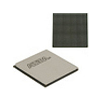
EP4SGX530HH35C2N Altera, EP4SGX530HH35C2N Datasheet - Page 261

EP4SGX530HH35C2N
Manufacturer Part Number
EP4SGX530HH35C2N
Description
IC STRATIX IV FPGA 530K 1152HBGA
Manufacturer
Altera
Series
Stratix® IV GXr
Datasheets
1.EP4SGX110DF29C3N.pdf
(80 pages)
2.EP4SGX110DF29C3N.pdf
(1154 pages)
3.EP4SGX110DF29C3N.pdf
(432 pages)
4.EP4SGX110DF29C3N.pdf
(22 pages)
5.EP4SGX110DF29C3N.pdf
(30 pages)
6.EP4SGX110DF29C3N.pdf
(72 pages)
7.EP4SGX530HH35C2N.pdf
(1145 pages)
Specifications of EP4SGX530HH35C2N
Number Of Logic Elements/cells
531200
Number Of Labs/clbs
21248
Total Ram Bits
27376
Number Of I /o
564
Voltage - Supply
0.87 V ~ 0.93 V
Mounting Type
Surface Mount
Operating Temperature
0°C ~ 85°C
Package / Case
1152-HBGA
Family Name
Stratix® IV
Number Of Logic Blocks/elements
531200
# Registers
424960
# I/os (max)
560
Process Technology
40nm
Operating Supply Voltage (typ)
900mV
Logic Cells
531200
Ram Bits
28033024
Operating Supply Voltage (min)
0.87V
Operating Supply Voltage (max)
0.93V
Operating Temp Range
0C to 85C
Operating Temperature Classification
Commercial
Mounting
Surface Mount
Pin Count
1152
Package Type
FCHBGA
Lead Free Status / RoHS Status
Lead free / RoHS Compliant
Number Of Gates
-
Lead Free Status / Rohs Status
Compliant
Available stocks
Company
Part Number
Manufacturer
Quantity
Price
- EP4SGX110DF29C3N PDF datasheet
- EP4SGX110DF29C3N PDF datasheet #2
- EP4SGX110DF29C3N PDF datasheet #3
- EP4SGX110DF29C3N PDF datasheet #4
- EP4SGX110DF29C3N PDF datasheet #5
- EP4SGX110DF29C3N PDF datasheet #6
- EP4SGX530HH35C2N PDF datasheet #7
- Current page: 261 of 432
- Download datasheet (11Mb)
Chapter 7: External Memory Interfaces in Stratix IV Devices
Stratix IV External Memory Interface Features
Figure 7–23. Simplified Diagram of the DQS Phase-Shift Circuitry
Notes to
(1) All features of the DQS phase-shift circuitry are accessible from the ALTMEMPHY megafunction in the Quartus II software.
(2) The input reference clock for the DQS phase-shift circuitry can come from a PLL output clock or an input clock pin. For more information, refer
(3) Phase offset settings can only go to the DQS logic blocks.
(4) DQS delay settings can go to the logic array, DQS logic block, and leveling circuitry.
February 2011 Altera Corporation
to
Input Reference
Table 7–5 on page 7–33
Clock (2)
Figure
7–23:
1
clk
DLL
Figure 7–23
into the DLL to a chain of up to 16 delay elements. The phase comparator compares
the signal coming out of the end of the delay chain block to the input reference clock.
The phase comparator then issues the upndn signal to the Gray-code counter. This
signal increments or decrements a six-bit delay setting (DQS delay settings) that
increases or decreases the delay through the delay element chain to bring the input
reference clock and the signals coming out of the delay element chain in phase.
In the Quartus II assignment, phase offset control block ‘A’ is designated as
DLLOFFSETCTRL_<coordinate x>_<coordinate y>_N1 and phase offset control block
‘B’ is designated as DLLOFFSETCTRL_<coordinate x>_<coordinate y>_N2.
You can reset the DLL from either the logic array or a user I/O pin. Each time the DLL
is reset, you must wait for 1,280 clock cycles for the DLL to lock before you can
capture the data properly.
Depending on the DLL frequency mode, the DLL can shift the incoming DQS signals
by 0°, 22.5°, 30°, 36°, 45°, 60°, 67.5°, 72°, 90°, 108°, 120°, 135°, 144°, 180°, or 240°. The
shifted DQS signal is then used as the clock for the DQ IOE input registers.
All DQS/CQ and CQn pins, referenced to the same DLL, can have their input signal
phase shifted by a different degree amount but all must be referenced at one
particular frequency. For example, you can have a 90° phase shift on DQS1T and a 60°
phase shift on DQS2T, referenced from a 200-MHz clock. Not all phase-shift
combinations are supported. The phase shifts on the DQS pins referenced by the same
DLL must all be a multiple of 22.5° (up to 90°), 30° (up to 120°), 36° (up to 144°), 45°
(up to 180°), or 60° (up to 240°).
Comparator
aload
through
Phase
Table 7–17 on page
Delay Chains
upndninclkena
upndnin
shows a simple block diagram of the DLL. The input reference clock goes
Up/Down
Counter
6
7–40.
6
offsetdelayctrlout [5:0]
offsetdelayctrlout [5:0]
delayctrlout [5:0]
dqsupdate
(Note 1)
offsetdelayctrlin [5:0]
offsetdelayctrlin [5:0]
6
DQS Delay
Settings
addnsub
addnsub
Phase offset settings
from the logic array
Phase offset settings
from the logic array
( offset [5:0] )
(4)
6
6
(dll_offset_ctrl_b)
(dll_offset_ctrl_a)
Control
Control
Phase
Phase
Offset
Offset
Stratix IV Device Handbook Volume 1
B
A
( offset [5:0] )
6
6
Phase offset
settings to DQS pin
on left or right edge (3)
( offsetctrlout [5:0] )
settings to DQS pins
on top or bottom edge (3)
Phase offset
( offsetctrlout [5:0] )
7–41
Related parts for EP4SGX530HH35C2N
Image
Part Number
Description
Manufacturer
Datasheet
Request
R

Part Number:
Description:
CYCLONE II STARTER KIT EP2C20N
Manufacturer:
Altera
Datasheet:

Part Number:
Description:
CPLD, EP610 Family, ECMOS Process, 300 Gates, 16 Macro Cells, 16 Reg., 16 User I/Os, 5V Supply, 35 Speed Grade, 24DIP
Manufacturer:
Altera Corporation
Datasheet:

Part Number:
Description:
CPLD, EP610 Family, ECMOS Process, 300 Gates, 16 Macro Cells, 16 Reg., 16 User I/Os, 5V Supply, 15 Speed Grade, 24DIP
Manufacturer:
Altera Corporation
Datasheet:

Part Number:
Description:
Manufacturer:
Altera Corporation
Datasheet:

Part Number:
Description:
CPLD, EP610 Family, ECMOS Process, 300 Gates, 16 Macro Cells, 16 Reg., 16 User I/Os, 5V Supply, 30 Speed Grade, 24DIP
Manufacturer:
Altera Corporation
Datasheet:

Part Number:
Description:
High-performance, low-power erasable programmable logic devices with 8 macrocells, 10ns
Manufacturer:
Altera Corporation
Datasheet:

Part Number:
Description:
High-performance, low-power erasable programmable logic devices with 8 macrocells, 7ns
Manufacturer:
Altera Corporation
Datasheet:

Part Number:
Description:
Classic EPLD
Manufacturer:
Altera Corporation
Datasheet:

Part Number:
Description:
High-performance, low-power erasable programmable logic devices with 8 macrocells, 10ns
Manufacturer:
Altera Corporation
Datasheet:

Part Number:
Description:
Manufacturer:
Altera Corporation
Datasheet:

Part Number:
Description:
Manufacturer:
Altera Corporation
Datasheet:

Part Number:
Description:
Manufacturer:
Altera Corporation
Datasheet:

Part Number:
Description:
CPLD, EP610 Family, ECMOS Process, 300 Gates, 16 Macro Cells, 16 Reg., 16 User I/Os, 5V Supply, 25 Speed Grade, 24DIP
Manufacturer:
Altera Corporation
Datasheet:


