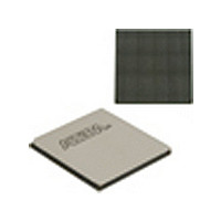
EP4SGX530HH35C2N Altera, EP4SGX530HH35C2N Datasheet - Page 173

EP4SGX530HH35C2N
Manufacturer Part Number
EP4SGX530HH35C2N
Description
IC STRATIX IV FPGA 530K 1152HBGA
Manufacturer
Altera
Series
Stratix® IV GXr
Datasheets
1.EP4SGX110DF29C3N.pdf
(80 pages)
2.EP4SGX110DF29C3N.pdf
(1154 pages)
3.EP4SGX110DF29C3N.pdf
(432 pages)
4.EP4SGX110DF29C3N.pdf
(22 pages)
5.EP4SGX110DF29C3N.pdf
(30 pages)
6.EP4SGX110DF29C3N.pdf
(72 pages)
7.EP4SGX530HH35C2N.pdf
(1145 pages)
Specifications of EP4SGX530HH35C2N
Number Of Logic Elements/cells
531200
Number Of Labs/clbs
21248
Total Ram Bits
27376
Number Of I /o
564
Voltage - Supply
0.87 V ~ 0.93 V
Mounting Type
Surface Mount
Operating Temperature
0°C ~ 85°C
Package / Case
1152-HBGA
Family Name
Stratix® IV
Number Of Logic Blocks/elements
531200
# Registers
424960
# I/os (max)
560
Process Technology
40nm
Operating Supply Voltage (typ)
900mV
Logic Cells
531200
Ram Bits
28033024
Operating Supply Voltage (min)
0.87V
Operating Supply Voltage (max)
0.93V
Operating Temp Range
0C to 85C
Operating Temperature Classification
Commercial
Mounting
Surface Mount
Pin Count
1152
Package Type
FCHBGA
Lead Free Status / RoHS Status
Lead free / RoHS Compliant
Number Of Gates
-
Lead Free Status / Rohs Status
Compliant
Available stocks
Company
Part Number
Manufacturer
Quantity
Price
- EP4SGX110DF29C3N PDF datasheet
- EP4SGX110DF29C3N PDF datasheet #2
- EP4SGX110DF29C3N PDF datasheet #3
- EP4SGX110DF29C3N PDF datasheet #4
- EP4SGX110DF29C3N PDF datasheet #5
- EP4SGX110DF29C3N PDF datasheet #6
- EP4SGX530HH35C2N PDF datasheet #7
- Current page: 173 of 432
- Download datasheet (11Mb)
© 2011 Altera Corporation. All rights reserved. ALTERA, ARRIA, CYCLONE, HARDCOPY, MAX, MEGACORE, NIOS, QUARTUS and STRATIX are Reg. U.S. Pat. & Tm. Off.
and/or trademarks of Altera Corporation in the U.S. and other countries. All other trademarks and service marks are the property of their respective holders as described at
www.altera.com/common/legal.html. Altera warrants performance of its semiconductor products to current specifications in accordance with Altera’s standard warranty, but
reserves the right to make changes to any products and services at any time without notice. Altera assumes no responsibility or liability arising out of the application or use of any
information, product, or service described herein except as expressly agreed to in writing by Altera. Altera customers are advised to obtain the latest version of device
specifications before relying on any published information and before placing orders for products or services.
SIV51006-3.2
Stratix IV Device Handbook Volume 1
February 2011
February 2011
SIV51006-3.2
This chapter describes how Stratix
you to work in compliance with current and emerging I/O standards and
requirements. With these device features, you can reduce board design interface costs
and increase development flexibility.
Altera
power efficiency for high-end applications, allowing you to innovate without
compromise. Stratix IV I/Os are specifically designed for ease-of-use and rapid
system integration while simultaneously providing the high bandwidth required to
maximize internal logic capabilities and produce system-level performance.
Stratix IV device I/O capability far exceeds the I/O bandwidth available from
previous generation FPGAs. Independent modular I/O banks with a common bank
structure for vertical migration lend efficiency and flexibility to the high-speed I/O.
Package and die enhancements with dynamic termination and output control provide
best-in-class signal integrity. Numerous I/O features assist high-speed data transfer
into and out of the device, including:
■
■
■
■
■
■
■
■
■
■
■
■
■
Up to 32 full-duplex clock data recovery (CDR)-based transceivers supporting
data rates between 600 Mbps and 8.5 Gbps
Dedicated circuitry to support physical layer functionality for popular serial
protocols, such as PCI Express
(GbE), Serial RapidIO
SD/HD/3G-SDI, Fibre Channel, SFI-5, and Interlaken
Complete PCIe protocol solution with embedded PCIe hard IP blocks that
implement PHY-MAC layer, data link layer, and transaction layer functionality
Single-ended, non-voltage-referenced, and voltage-referenced I/O standards
Low-voltage differential signaling (LVDS), reduced swing differential signaling
(RSDS), mini-LVDS, high-speed transceiver logic (HSTL), and SSTL
Single data rate (SDR) and half data rate (HDR—half frequency and twice data
width of SDR) input and output options
Up to 132 full duplex 1.6 Gbps true LVDS channels (132 Tx + 132 Rx) on the row
I/O banks
Hard dynamic phase alignment (DPA) block with serializer/deserializer
(SERDES)
Deskew, read and write leveling, and clock-domain crossing functionality
Programmable output current strength
Programmable slew rate
Programmable delay
Programmable bus-hold circuit
®
Stratix IV FPGAs deliver a breakthrough level of system bandwidth and
®
, SONET/SDH, XAUI/HiGig, (OIF) CEI-6G,
6. I/O Features in Stratix IV Devices
®
®
(PIPE) (PCIe) Gen1 and Gen2, Gigabit Ethernet
IV devices provide I/O capabilities that allow
Subscribe
Related parts for EP4SGX530HH35C2N
Image
Part Number
Description
Manufacturer
Datasheet
Request
R

Part Number:
Description:
CYCLONE II STARTER KIT EP2C20N
Manufacturer:
Altera
Datasheet:

Part Number:
Description:
CPLD, EP610 Family, ECMOS Process, 300 Gates, 16 Macro Cells, 16 Reg., 16 User I/Os, 5V Supply, 35 Speed Grade, 24DIP
Manufacturer:
Altera Corporation
Datasheet:

Part Number:
Description:
CPLD, EP610 Family, ECMOS Process, 300 Gates, 16 Macro Cells, 16 Reg., 16 User I/Os, 5V Supply, 15 Speed Grade, 24DIP
Manufacturer:
Altera Corporation
Datasheet:

Part Number:
Description:
Manufacturer:
Altera Corporation
Datasheet:

Part Number:
Description:
CPLD, EP610 Family, ECMOS Process, 300 Gates, 16 Macro Cells, 16 Reg., 16 User I/Os, 5V Supply, 30 Speed Grade, 24DIP
Manufacturer:
Altera Corporation
Datasheet:

Part Number:
Description:
High-performance, low-power erasable programmable logic devices with 8 macrocells, 10ns
Manufacturer:
Altera Corporation
Datasheet:

Part Number:
Description:
High-performance, low-power erasable programmable logic devices with 8 macrocells, 7ns
Manufacturer:
Altera Corporation
Datasheet:

Part Number:
Description:
Classic EPLD
Manufacturer:
Altera Corporation
Datasheet:

Part Number:
Description:
High-performance, low-power erasable programmable logic devices with 8 macrocells, 10ns
Manufacturer:
Altera Corporation
Datasheet:

Part Number:
Description:
Manufacturer:
Altera Corporation
Datasheet:

Part Number:
Description:
Manufacturer:
Altera Corporation
Datasheet:

Part Number:
Description:
Manufacturer:
Altera Corporation
Datasheet:

Part Number:
Description:
CPLD, EP610 Family, ECMOS Process, 300 Gates, 16 Macro Cells, 16 Reg., 16 User I/Os, 5V Supply, 25 Speed Grade, 24DIP
Manufacturer:
Altera Corporation
Datasheet:


