DK-DEV-4SGX230N Altera, DK-DEV-4SGX230N Datasheet - Page 125
DK-DEV-4SGX230N
Manufacturer Part Number
DK-DEV-4SGX230N
Description
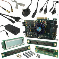
KIT DEVELOPMENT STRATIX IV
Manufacturer
Altera
Series
Stratix® IVr
Type
FPGAr
Datasheets
1.EP4SGX110DF29C3N.pdf
(80 pages)
2.EP4SGX110DF29C3N.pdf
(1154 pages)
3.DK-DEV-4SGX230N.pdf
(2 pages)
4.DK-DEV-4SGX530N.pdf
(57 pages)
Specifications of DK-DEV-4SGX230N
Contents
Development Board, Universal Power Supply, Cables and Software
Silicon Manufacturer
Altera
Core Architecture
FPGA
Core Sub-architecture
Stratix
Silicon Core Number
EP4S
Silicon Family Name
Stratix IV GX
Rohs Compliant
Yes
For Use With/related Products
EP4SGX230K
Lead Free Status / RoHS Status
Lead free / RoHS Compliant
Other names
544-2594
Available stocks
Company
Part Number
Manufacturer
Quantity
Price
Company:

Part Number:
DK-DEV-4SGX230N
Manufacturer:
Altera
Quantity:
135


Chapter 5: Clock Networks and PLLs in Stratix IV Devices
Clock Networks in Stratix IV Devices
February 2011 Altera Corporation
Clock Sources Per Quadrant
Clock Regions
1
There are 26 section clock (SCLK) networks available in each spine clock that can
drive six row clocks in each logic array block (LAB) row, nine column I/O clocks, and
three core reference clocks. The SCLKs are the clock resources to the core functional
blocks, PLLs, and I/O interfaces of the device.
be driven by the GCLK, RCLK, PCLK, or the PLL feedback clock networks in each
spine clock.
A spine clock is another layer of routing below the GCLKs, RCLKs, and PCLKs before
each clock is connected to clock routing for each LAB row. The settings for spine
clocks are transparent to all users. The Quartus II software automatically routes the
spine clock based on the GCLK, RCLK, and PCLKs.
Figure 5–9. Hierarchical Clock Networks per Spine Clock
Notes to
(1) The GCLK, RCLK, PCLK, and PLL feedback clocks share the same routing to the SCLKs. The total number of clock
(2) There are up to 16 PCLKs that can drive the SCLKs in each spine clock in the largest device.
(3) There are up to 22 RCLKs that can drive the SCLKs in each spine clock in the largest device.
(4) The PLL feedback clock is the clock from the PLL that drives into the SCLKs.
(5) The column I/O clock is the clock that drives the column I/O core registers and I/O interfaces.
(6) The core reference clock is the clock that feeds into the PLL as the PLL reference clock.
(7) The row clock is the clock source to the LAB, memory blocks, and row I/O interfaces in the core row.
Stratix IV devices provide up to 104 distinct clock domains (16 GCLKs + 88 RCLKs) in
the entire device. You can use these clock resources to form the following types of
clock regions:
■
■
■
To form the entire device clock region, a source (not necessarily a clock signal) drives a
GCLK network that can be routed through the entire device. This clock region has the
maximum delay when compared with other clock regions, but allows the signal to
reach every destination within the device. This is a good option for routing global
reset and clear signals or routing clocks throughout the device.
PLL feedback clock
Entire device
Regional
Dual-regional
resources must not exceed the SCLK limits in each region to ensure successful design fitting in the Quartus II
software.
Figure
5–9:
GCLK
RCLK
PCLK
(4)
16
16 (2)
22 (3)
3
SCLK
Figure 5–9
26
(Note 1)
shows that the SCLKs can
Stratix IV Device Handbook Volume 1
9
3
6
Column I/O clock
Core reference clock
Row clock
(7)
5–9
(5)
(6)
Related parts for DK-DEV-4SGX230N
Image
Part Number
Description
Manufacturer
Datasheet
Request
R

Part Number:
Description:
KIT DEV ARRIA II GX FPGA 2AGX125
Manufacturer:
Altera
Datasheet:

Part Number:
Description:
KIT DEV CYCLONE III LS EP3CLS200
Manufacturer:
Altera
Datasheet:

Part Number:
Description:
KIT DEV STRATIX IV FPGA 4SE530
Manufacturer:
Altera
Datasheet:

Part Number:
Description:
KIT DEV FPGA 2AGX260 W/6.375G TX
Manufacturer:
Altera
Datasheet:

Part Number:
Description:
KIT DEV MAX V 5M570Z
Manufacturer:
Altera
Datasheet:

Part Number:
Description:
KIT DEV STRATIX V FPGA 5SGXEA7
Manufacturer:
Altera
Datasheet:

Part Number:
Description:
KIT DEVELOPMENT STRATIX III
Manufacturer:
Altera
Datasheet:

Part Number:
Description:
KIT DEV ARRIA GX 1AGX60N
Manufacturer:
Altera
Datasheet:
Part Number:
Description:
KIT STARTER CYCLONE IV GX
Manufacturer:
Altera
Datasheet:
Part Number:
Description:
KIT DEVELOPMENT STRATIX IV
Manufacturer:
Altera
Datasheet:

Part Number:
Description:
CPLD, EP610 Family, ECMOS Process, 300 Gates, 16 Macro Cells, 16 Reg., 16 User I/Os, 5V Supply, 35 Speed Grade, 24DIP
Manufacturer:
Altera Corporation
Datasheet:
Part Number:
Description:
CPLD, EP610 Family, ECMOS Process, 300 Gates, 16 Macro Cells, 16 Reg., 16 User I/Os, 5V Supply, 15 Speed Grade, 24DIP
Manufacturer:
Altera Corporation
Datasheet: