DK-DEV-4SGX230N Altera, DK-DEV-4SGX230N Datasheet - Page 301
DK-DEV-4SGX230N
Manufacturer Part Number
DK-DEV-4SGX230N
Description
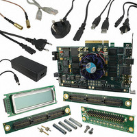
KIT DEVELOPMENT STRATIX IV
Manufacturer
Altera
Series
Stratix® IVr
Type
FPGAr
Datasheets
1.EP4SGX110DF29C3N.pdf
(80 pages)
2.EP4SGX110DF29C3N.pdf
(1154 pages)
3.DK-DEV-4SGX230N.pdf
(2 pages)
4.DK-DEV-4SGX530N.pdf
(57 pages)
Specifications of DK-DEV-4SGX230N
Contents
Development Board, Universal Power Supply, Cables and Software
Silicon Manufacturer
Altera
Core Architecture
FPGA
Core Sub-architecture
Stratix
Silicon Core Number
EP4S
Silicon Family Name
Stratix IV GX
Rohs Compliant
Yes
For Use With/related Products
EP4SGX230K
Lead Free Status / RoHS Status
Lead free / RoHS Compliant
Other names
544-2594
Available stocks
Company
Part Number
Manufacturer
Quantity
Price
Company:

Part Number:
DK-DEV-4SGX230N
Manufacturer:
Altera
Quantity:
135


Chapter 8: High-Speed Differential I/O Interfaces and DPA in Stratix IV Devices
Differential Receiver
Figure 8–18. Receiver Data Path in Non-DPA Mode
Notes to
(1) In SDR and DDR modes, the data width from the IOE is 1 and 2 bits, respectively.
(2) The rx_out port has a maximum data width of 10 bits.
February 2011 Altera Corporation
rx_divfwdclk
rx_outclock
Fabric
FPGA
Figure
rx_out
8–18:
f
1
10
When using non-DPA receivers, you must drive the PLL from a dedicated and
compensated clock input pin. Compensated clock inputs are dedicated clock pins in
the same I/O bank as the PLL.
For more information about dedicated and compensated clock inputs, refer to the
Clock Networks and PLLs in Stratix IV Devices
IOE Supports SDR, DDR, or Non-Registered Datapath
(LOAD_EN, diffioclk)
2
Deserializer
DOUT DIN
IOE
2
Left/Right PLL
3
DOUT DIN
Clock Mux
Bit Slip
(LVDS_LOAD_EN,
(Note
LVDS_diffioclk,
rx_outclk)
diffioclk
1),
(2)
rx_inclock
chapter.
8 Serial LVDS
Clock Phases
Synchronizer
DOUT DIN
L L
LVDS Receiver
N
3
(DPA_LO
Stratix IV Device Handbook Volume 1
DPA_diffioclk,
rx_divfwdclk)
P P
P P
AD_EN,
DPA Circuitr
Retimed
DPA Cloc
LVDS Clock Domain
P P
P P
Data
k
DIN
y
+
rx_in
8–23
Related parts for DK-DEV-4SGX230N
Image
Part Number
Description
Manufacturer
Datasheet
Request
R

Part Number:
Description:
KIT DEV ARRIA II GX FPGA 2AGX125
Manufacturer:
Altera
Datasheet:

Part Number:
Description:
KIT DEV CYCLONE III LS EP3CLS200
Manufacturer:
Altera
Datasheet:

Part Number:
Description:
KIT DEV STRATIX IV FPGA 4SE530
Manufacturer:
Altera
Datasheet:

Part Number:
Description:
KIT DEV FPGA 2AGX260 W/6.375G TX
Manufacturer:
Altera
Datasheet:

Part Number:
Description:
KIT DEV MAX V 5M570Z
Manufacturer:
Altera
Datasheet:

Part Number:
Description:
KIT DEV STRATIX V FPGA 5SGXEA7
Manufacturer:
Altera
Datasheet:

Part Number:
Description:
KIT DEVELOPMENT STRATIX III
Manufacturer:
Altera
Datasheet:

Part Number:
Description:
KIT DEV ARRIA GX 1AGX60N
Manufacturer:
Altera
Datasheet:
Part Number:
Description:
KIT STARTER CYCLONE IV GX
Manufacturer:
Altera
Datasheet:
Part Number:
Description:
KIT DEVELOPMENT STRATIX IV
Manufacturer:
Altera
Datasheet:

Part Number:
Description:
CPLD, EP610 Family, ECMOS Process, 300 Gates, 16 Macro Cells, 16 Reg., 16 User I/Os, 5V Supply, 35 Speed Grade, 24DIP
Manufacturer:
Altera Corporation
Datasheet:
Part Number:
Description:
CPLD, EP610 Family, ECMOS Process, 300 Gates, 16 Macro Cells, 16 Reg., 16 User I/Os, 5V Supply, 15 Speed Grade, 24DIP
Manufacturer:
Altera Corporation
Datasheet: