DK-DEV-4SGX230N Altera, DK-DEV-4SGX230N Datasheet - Page 267
DK-DEV-4SGX230N
Manufacturer Part Number
DK-DEV-4SGX230N
Description
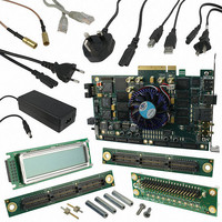
KIT DEVELOPMENT STRATIX IV
Manufacturer
Altera
Series
Stratix® IVr
Type
FPGAr
Datasheets
1.EP4SGX110DF29C3N.pdf
(80 pages)
2.EP4SGX110DF29C3N.pdf
(1154 pages)
3.DK-DEV-4SGX230N.pdf
(2 pages)
4.DK-DEV-4SGX530N.pdf
(57 pages)
Specifications of DK-DEV-4SGX230N
Contents
Development Board, Universal Power Supply, Cables and Software
Silicon Manufacturer
Altera
Core Architecture
FPGA
Core Sub-architecture
Stratix
Silicon Core Number
EP4S
Silicon Family Name
Stratix IV GX
Rohs Compliant
Yes
For Use With/related Products
EP4SGX230K
Lead Free Status / RoHS Status
Lead free / RoHS Compliant
Other names
544-2594
Available stocks
Company
Part Number
Manufacturer
Quantity
Price
Company:

Part Number:
DK-DEV-4SGX230N
Manufacturer:
Altera
Quantity:
135


Chapter 7: External Memory Interfaces in Stratix IV Devices
Stratix IV External Memory Interface Features
February 2011 Altera Corporation
Leveling Circuitry
DDR3 SDRAM unbuffered modules use a fly-by clock distribution topology for better
signal integrity. This means that the CK/CK# signals arrive at each DDR3 SDRAM
device in the module at different times. The difference in arrival time between the first
DDR3 SDRAM device and the last device on the module can be as long as 1.6 ns.
Figure 7–27
Figure 7–27. DDR3 SDRAM Unbuffered Module Clock Topology
Because the data and read strobe signals are still point-to-point, take special care to
ensure that the timing relationship between the CK/CK# and DQS signals (tDQSS,
tDSS, and tDSH) during a write is met at every device on the modules. Furthermore,
read data coming back into the FPGA from the memory is also staggered in a similar
way.
Stratix IV FPGAs have leveling circuitry to address these two situations. There is one
leveling circuitry per I/O sub-bank (for example, I/O sub-bank 1A, 1B, and 1C each
has one leveling circuitry). These delay chains are PVT-compensated by the same DQS
delay settings as the DLL and DQS delay chains.
For frequencies equal to and above 400 MHz, the DLL uses eight delay chains, such
that each delay chain generates a 45° delay. The generated clock phases are
distributed to every DQS logic block that is available in the I/O sub-bank. The delay
chain taps then feeds a multiplexer controlled by the ALTMEMPHY megafunction to
select which clock phases are to be used for that ×4 or × 8 DQS group. Each group can
use a different tap output from the read-leveling and write-leveling delay chains to
compensate for the different CK/CK# delay going into each device on the module.
DQS/DQ
shows the clock topology in DDR3 SDRAM unbuffered modules.
DQS/DQ
DQS/DQ
DQS/DQ
CK/CK#
DQS/DQ
DQS/DQ
Stratix IV Device Handbook Volume 1
DQS/DQ
Stratix IV Device
DQS/DQ
7–47
Related parts for DK-DEV-4SGX230N
Image
Part Number
Description
Manufacturer
Datasheet
Request
R

Part Number:
Description:
KIT DEV ARRIA II GX FPGA 2AGX125
Manufacturer:
Altera
Datasheet:

Part Number:
Description:
KIT DEV CYCLONE III LS EP3CLS200
Manufacturer:
Altera
Datasheet:

Part Number:
Description:
KIT DEV STRATIX IV FPGA 4SE530
Manufacturer:
Altera
Datasheet:

Part Number:
Description:
KIT DEV FPGA 2AGX260 W/6.375G TX
Manufacturer:
Altera
Datasheet:

Part Number:
Description:
KIT DEV MAX V 5M570Z
Manufacturer:
Altera
Datasheet:

Part Number:
Description:
KIT DEV STRATIX V FPGA 5SGXEA7
Manufacturer:
Altera
Datasheet:

Part Number:
Description:
KIT DEVELOPMENT STRATIX III
Manufacturer:
Altera
Datasheet:

Part Number:
Description:
KIT DEV ARRIA GX 1AGX60N
Manufacturer:
Altera
Datasheet:
Part Number:
Description:
KIT STARTER CYCLONE IV GX
Manufacturer:
Altera
Datasheet:
Part Number:
Description:
KIT DEVELOPMENT STRATIX IV
Manufacturer:
Altera
Datasheet:

Part Number:
Description:
CPLD, EP610 Family, ECMOS Process, 300 Gates, 16 Macro Cells, 16 Reg., 16 User I/Os, 5V Supply, 35 Speed Grade, 24DIP
Manufacturer:
Altera Corporation
Datasheet:
Part Number:
Description:
CPLD, EP610 Family, ECMOS Process, 300 Gates, 16 Macro Cells, 16 Reg., 16 User I/Os, 5V Supply, 15 Speed Grade, 24DIP
Manufacturer:
Altera Corporation
Datasheet: