DK-DEV-4SGX230N Altera, DK-DEV-4SGX230N Datasheet - Page 144
DK-DEV-4SGX230N
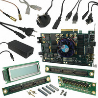
Manufacturer Part Number
DK-DEV-4SGX230N
Description
KIT DEVELOPMENT STRATIX IV
Manufacturer
Altera
Series
Stratix® IVr
Type
FPGAr
Datasheets
1.EP4SGX110DF29C3N.pdf
(80 pages)
2.EP4SGX110DF29C3N.pdf
(1154 pages)
3.DK-DEV-4SGX230N.pdf
(2 pages)
4.DK-DEV-4SGX530N.pdf
(57 pages)
Specifications of DK-DEV-4SGX230N
Contents
Development Board, Universal Power Supply, Cables and Software
Silicon Manufacturer
Altera
Core Architecture
FPGA
Core Sub-architecture
Stratix
Silicon Core Number
EP4S
Silicon Family Name
Stratix IV GX
Rohs Compliant
Yes
For Use With/related Products
EP4SGX230K
Lead Free Status / RoHS Status
Lead free / RoHS Compliant
Other names
544-2594
Available stocks
Company
Part Number
Manufacturer
Quantity
Price
Company:

Part Number:
DK-DEV-4SGX230N
Manufacturer:
Altera
Quantity:
135


5–28
Stratix IV Device Handbook Volume 1
Source Synchronous Mode
If data and clock arrive at the same time on the input pins, the same phase
relationship is maintained at the clock and data ports of any IOE input register.
Figure 5–22
recommends source synchronous mode for source-synchronous data transfers. Data
and clock signals at the IOE experience similar buffer delays as long as you use the
same I/O standard.
Figure 5–22. Phase Relationship Between Clock and Data in Source-Synchronous Mode
Source-synchronous mode compensates for the delay of the clock network used plus
any difference in the delay between these two paths:
■
■
The Stratix IV PLL can compensate multiple pad-to-input-register paths, such as a
data bus when it is set to use source-synchronous compensation mode. You can use
the “PLL Compensation” assignment in the Quartus II software Assignment Editor to
select which input pins are used as the PLL compensation targets. You can include
your entire data bus, provided the input registers are clocked by the same output of a
source-synchronous-compensated PLL. In order for the clock delay to be properly
compensated, all of the input pins must be on the same side of the device. The PLL
compensates for the input pin with the longest pad-to-register delay among all input
pins in the compensated bus.
If you do not make the “PLL Compensation” assignment, the Quartus II software
automatically selects all of the pins driven by the compensated output of the PLL as
the compensation target.
Data pin to the IOE register input
Clock input pin to the PLL PFD input
shows an example waveform of the clock and data in this mode. Altera
Clock at register
Data at register
reference clock
at input pin
Data pin
PLL
Chapter 5: Clock Networks and PLLs in Stratix IV Devices
February 2011 Altera Corporation
PLLs in Stratix IV Devices
Related parts for DK-DEV-4SGX230N
Image
Part Number
Description
Manufacturer
Datasheet
Request
R

Part Number:
Description:
KIT DEV ARRIA II GX FPGA 2AGX125
Manufacturer:
Altera
Datasheet:

Part Number:
Description:
KIT DEV CYCLONE III LS EP3CLS200
Manufacturer:
Altera
Datasheet:

Part Number:
Description:
KIT DEV STRATIX IV FPGA 4SE530
Manufacturer:
Altera
Datasheet:

Part Number:
Description:
KIT DEV FPGA 2AGX260 W/6.375G TX
Manufacturer:
Altera
Datasheet:

Part Number:
Description:
KIT DEV MAX V 5M570Z
Manufacturer:
Altera
Datasheet:

Part Number:
Description:
KIT DEV STRATIX V FPGA 5SGXEA7
Manufacturer:
Altera
Datasheet:

Part Number:
Description:
KIT DEVELOPMENT STRATIX III
Manufacturer:
Altera
Datasheet:

Part Number:
Description:
KIT DEV ARRIA GX 1AGX60N
Manufacturer:
Altera
Datasheet:
Part Number:
Description:
KIT STARTER CYCLONE IV GX
Manufacturer:
Altera
Datasheet:
Part Number:
Description:
KIT DEVELOPMENT STRATIX IV
Manufacturer:
Altera
Datasheet:

Part Number:
Description:
CPLD, EP610 Family, ECMOS Process, 300 Gates, 16 Macro Cells, 16 Reg., 16 User I/Os, 5V Supply, 35 Speed Grade, 24DIP
Manufacturer:
Altera Corporation
Datasheet:
Part Number:
Description:
CPLD, EP610 Family, ECMOS Process, 300 Gates, 16 Macro Cells, 16 Reg., 16 User I/Os, 5V Supply, 15 Speed Grade, 24DIP
Manufacturer:
Altera Corporation
Datasheet: