DK-DEV-4SGX230N Altera, DK-DEV-4SGX230N Datasheet - Page 228
DK-DEV-4SGX230N
Manufacturer Part Number
DK-DEV-4SGX230N
Description
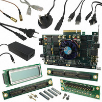
KIT DEVELOPMENT STRATIX IV
Manufacturer
Altera
Series
Stratix® IVr
Type
FPGAr
Datasheets
1.EP4SGX110DF29C3N.pdf
(80 pages)
2.EP4SGX110DF29C3N.pdf
(1154 pages)
3.DK-DEV-4SGX230N.pdf
(2 pages)
4.DK-DEV-4SGX530N.pdf
(57 pages)
Specifications of DK-DEV-4SGX230N
Contents
Development Board, Universal Power Supply, Cables and Software
Silicon Manufacturer
Altera
Core Architecture
FPGA
Core Sub-architecture
Stratix
Silicon Core Number
EP4S
Silicon Family Name
Stratix IV GX
Rohs Compliant
Yes
For Use With/related Products
EP4SGX230K
Lead Free Status / RoHS Status
Lead free / RoHS Compliant
Other names
544-2594
Available stocks
Company
Part Number
Manufacturer
Quantity
Price
Company:

Part Number:
DK-DEV-4SGX230N
Manufacturer:
Altera
Quantity:
135


7–8
Figure 7–3. Number of DQS/DQ Groups per Bank in EP4SGX70, EP4SGX110, EP4SGX180, and EP4SGX230 Devices in the
780-Pin FineLine BGA Package
Notes to
(1) These numbers are preliminary until the devices are available.
(2) EP4SGX70, EP4SGX110, EP4SGX180, and EP4SGX230 devices do not support ×32/×36 mode. To interface with a ×36 QDR II+/QDR II SRAM
(3) You can also use DQS/DQSn pins in some of the ×4 groups as R
(4) You can also use some of the DQS/DQ pins in I/O Bank 1C as configuration pins. You cannot use a ×4 DQS/DQ group with any of its pin members
(5) All I/O pin counts include dedicated clock inputs that you can use for data inputs.
Stratix IV Device Handbook Volume 1
device, refer to
of the ×4 group are used as R
can use the ×16/×18 or ×32/×36 groups that include that ×4 group; however, there are restrictions on using ×8/×9 groups that include that ×4
group.
used for configuration purposes. Ensure that the DQS/DQ groups that you have chosen are not also used for configuration because you may lose
up to four ×4 DQS/DQ groups, depending on your configuration scheme.
Figure
7–3:
“Combining ×16/×18 DQS/DQ Groups for a ×36 QDR II+/QDR II SRAM Interface” on page
26 User I/Os
26 User I/Os
32 User I/Os
I/O Bank 2C
I/O Bank 2A
I/O Bank 1C
x16/x18=0
32 User I/Os
x16/x18=0
x16/x18=1
I/O Bank 1A
x16/x18=1
x8/x9=1
x8/x9=1
x8/x9=2
x8/x9=2
DLL0
x4=3
x4=3
x4=4
DLL1
x4=4
UP
and R
(Note
I/O Bank 8A
40 User I/Os
I/O Bank 3A
40 User I/Os
x16/x18=1
x16/x18=1
x8/x9=3
x8/x9=3
DN
x4=6
x4=6
pins for OCT calibration. If two pins of a ×4 group are used as R
1), (2), (3), (4).
24 User I/Os
I/O Bank 8C
x16/x18=0
I/O Bank 3C
24 User I/Os
x8/x9=1
EP4SGX70, EP4SGX110, EP4SGX180, and
x16/x18=0
x4=2
x8/x9=1
x4=2
EP4SGX230 Devices in the
780-Pin FineLine BGA
UP
(5)
and R
24 User I/Os
I/O Bank 7C
24 User I/Os
x16/x18=0
I/O Bank 4C
x16/x18=0
DN
x8/x9=1
x8/x9=1
x4=3
x4=3
pins, but you cannot use a ×4 group for memory interfaces if two pins
Chapter 7: External Memory Interfaces in Stratix IV Devices
40 User I/Os
I/O Bank 7A
I/O Bank 4A
40 User I/Os
x16/x18=1
x16/x18=1
x8/x9=3
x8/x9=3
x4=6
x4=6
UP
7–26.
and R
DLL3
February 2011 Altera Corporation
DLL2
Memory Interfaces Pin Support
DN
pins for OCT calibration, you
Related parts for DK-DEV-4SGX230N
Image
Part Number
Description
Manufacturer
Datasheet
Request
R

Part Number:
Description:
KIT DEV ARRIA II GX FPGA 2AGX125
Manufacturer:
Altera
Datasheet:

Part Number:
Description:
KIT DEV CYCLONE III LS EP3CLS200
Manufacturer:
Altera
Datasheet:

Part Number:
Description:
KIT DEV STRATIX IV FPGA 4SE530
Manufacturer:
Altera
Datasheet:

Part Number:
Description:
KIT DEV FPGA 2AGX260 W/6.375G TX
Manufacturer:
Altera
Datasheet:

Part Number:
Description:
KIT DEV MAX V 5M570Z
Manufacturer:
Altera
Datasheet:

Part Number:
Description:
KIT DEV STRATIX V FPGA 5SGXEA7
Manufacturer:
Altera
Datasheet:

Part Number:
Description:
KIT DEVELOPMENT STRATIX III
Manufacturer:
Altera
Datasheet:

Part Number:
Description:
KIT DEV ARRIA GX 1AGX60N
Manufacturer:
Altera
Datasheet:
Part Number:
Description:
KIT STARTER CYCLONE IV GX
Manufacturer:
Altera
Datasheet:
Part Number:
Description:
KIT DEVELOPMENT STRATIX IV
Manufacturer:
Altera
Datasheet:

Part Number:
Description:
CPLD, EP610 Family, ECMOS Process, 300 Gates, 16 Macro Cells, 16 Reg., 16 User I/Os, 5V Supply, 35 Speed Grade, 24DIP
Manufacturer:
Altera Corporation
Datasheet:
Part Number:
Description:
CPLD, EP610 Family, ECMOS Process, 300 Gates, 16 Macro Cells, 16 Reg., 16 User I/Os, 5V Supply, 15 Speed Grade, 24DIP
Manufacturer:
Altera Corporation
Datasheet: