DK-DEV-4SGX230N Altera, DK-DEV-4SGX230N Datasheet - Page 460
DK-DEV-4SGX230N
Manufacturer Part Number
DK-DEV-4SGX230N
Description
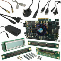
KIT DEVELOPMENT STRATIX IV
Manufacturer
Altera
Series
Stratix® IVr
Type
FPGAr
Datasheets
1.EP4SGX110DF29C3N.pdf
(80 pages)
2.EP4SGX110DF29C3N.pdf
(1154 pages)
3.DK-DEV-4SGX230N.pdf
(2 pages)
4.DK-DEV-4SGX530N.pdf
(57 pages)
Specifications of DK-DEV-4SGX230N
Contents
Development Board, Universal Power Supply, Cables and Software
Silicon Manufacturer
Altera
Core Architecture
FPGA
Core Sub-architecture
Stratix
Silicon Core Number
EP4S
Silicon Family Name
Stratix IV GX
Rohs Compliant
Yes
For Use With/related Products
EP4SGX230K
Lead Free Status / RoHS Status
Lead free / RoHS Compliant
Other names
544-2594
Available stocks
Company
Part Number
Manufacturer
Quantity
Price
Company:

Part Number:
DK-DEV-4SGX230N
Manufacturer:
Altera
Quantity:
135


1–16
Transceiver Block Architecture
Figure 1–11. Top-Level View of a Transceiver Block
Stratix IV Device Handbook Volume 2: Transceivers
Transceiver Block
Transceiver Block
Channel 3
Channel 2
Channel 1
Channel 0
Channel 3
Channel 2
Channel 1
Channel 0
QL1
QL0
Figure 1–11
Each transceiver block has the following components:
1. Four full-duplex (transmitter and receiver) transceiver channels that support serial
2. Two CMU channels—CMU0 and CMU1 channels—that provide the high-speed serial
3. Central control unit (CCU) that implements the XAUI state machine for
data rates from 600 Mbps to 8.5 Gbps in Stratix IV GX devices and 600 Mbps to
11.3 Gbps in Stratix IV GT devices. For more information, refer to
Channel Architecture” on page
and low-speed parallel clock to the transceiver channels. For more information,
refer to
XGMII-to-PCS code group conversion, XAUI deskew state machine, shared
control signal generation block, PCIe rateswitch controller block, and reset control
logic
■
■
The shared control signal generation block provides control signals to the
transceiver channels in bonded functional modes, such as XAUI, PCIe, and
Basic ×4.
The PCIe rateswitch controller block controls the rateswitch circuit in the CMU0
channel in ×4 configurations. In PCIe ×8 configuration, the PCIe rateswitch
controller block of the CCU in the master transceiver block is active. For more
information, refer to
“CMU Channel Architecture” on page
shows the transceiver block architecture of Stratix GX and GT devices.
Transceiver Block
Transceiver Block
QR1
QR0
Channel 3
Channel 2
Channel 1
Channel 0
Channel 3
Channel 2
Channel 1
Channel 0
“PCIe Gen2 (5 Gbps) Support” on page
1–17.
Chapter 1: Transceiver Architecture in Stratix IV Devices
Unit (CCU)
Central
Control
Transceiver Channel 3
Transceiver Channel 2
Transceiver Channel 1
Transceiver Channel 0
3
Transceiver Block
1–100.
CMU1 Channel
CMU0 Channel
February 2011 Altera Corporation
1
Transceiver Block Architecture
1
1
1
1–140.
2
2
“Transceiver
Related parts for DK-DEV-4SGX230N
Image
Part Number
Description
Manufacturer
Datasheet
Request
R

Part Number:
Description:
KIT DEV ARRIA II GX FPGA 2AGX125
Manufacturer:
Altera
Datasheet:

Part Number:
Description:
KIT DEV CYCLONE III LS EP3CLS200
Manufacturer:
Altera
Datasheet:

Part Number:
Description:
KIT DEV STRATIX IV FPGA 4SE530
Manufacturer:
Altera
Datasheet:

Part Number:
Description:
KIT DEV FPGA 2AGX260 W/6.375G TX
Manufacturer:
Altera
Datasheet:

Part Number:
Description:
KIT DEV MAX V 5M570Z
Manufacturer:
Altera
Datasheet:

Part Number:
Description:
KIT DEV STRATIX V FPGA 5SGXEA7
Manufacturer:
Altera
Datasheet:

Part Number:
Description:
KIT DEVELOPMENT STRATIX III
Manufacturer:
Altera
Datasheet:

Part Number:
Description:
KIT DEV ARRIA GX 1AGX60N
Manufacturer:
Altera
Datasheet:
Part Number:
Description:
KIT STARTER CYCLONE IV GX
Manufacturer:
Altera
Datasheet:
Part Number:
Description:
KIT DEVELOPMENT STRATIX IV
Manufacturer:
Altera
Datasheet:

Part Number:
Description:
CPLD, EP610 Family, ECMOS Process, 300 Gates, 16 Macro Cells, 16 Reg., 16 User I/Os, 5V Supply, 35 Speed Grade, 24DIP
Manufacturer:
Altera Corporation
Datasheet:
Part Number:
Description:
CPLD, EP610 Family, ECMOS Process, 300 Gates, 16 Macro Cells, 16 Reg., 16 User I/Os, 5V Supply, 15 Speed Grade, 24DIP
Manufacturer:
Altera Corporation
Datasheet: