DK-DEV-4SGX230N Altera, DK-DEV-4SGX230N Datasheet - Page 372
DK-DEV-4SGX230N
Manufacturer Part Number
DK-DEV-4SGX230N
Description
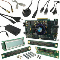
KIT DEVELOPMENT STRATIX IV
Manufacturer
Altera
Series
Stratix® IVr
Type
FPGAr
Datasheets
1.EP4SGX110DF29C3N.pdf
(80 pages)
2.EP4SGX110DF29C3N.pdf
(1154 pages)
3.DK-DEV-4SGX230N.pdf
(2 pages)
4.DK-DEV-4SGX530N.pdf
(57 pages)
Specifications of DK-DEV-4SGX230N
Contents
Development Board, Universal Power Supply, Cables and Software
Silicon Manufacturer
Altera
Core Architecture
FPGA
Core Sub-architecture
Stratix
Silicon Core Number
EP4S
Silicon Family Name
Stratix IV GX
Rohs Compliant
Yes
For Use With/related Products
EP4SGX230K
Lead Free Status / RoHS Status
Lead free / RoHS Compliant
Other names
544-2594
Available stocks
Company
Part Number
Manufacturer
Quantity
Price
Company:

Part Number:
DK-DEV-4SGX230N
Manufacturer:
Altera
Quantity:
135


10–38
Figure 10–17. JTAG Configuration of Multiple Devices Using a Download Cable
Notes to
(1) Connect the pull-up resistor to the same supply voltage as the USB Blaster, MasterBlaster (V
(2) Connect the nCONFIG and MSEL[2..0] pins to support a non-JTAG configuration scheme. If you only use a JTAG configuration, connect
(3) Pin 6 of the header is a V
(4) You must connect nCE to GND or drive it low for successful JTAG configuration.
(5) The pull-up resistor value can vary from 1 k to 10 kΩ.
Stratix IV Device Handbook Volume 1
Pin 1
EthernetBlaster cable. Connect the voltage supply to V
nCONFIG to V
this value, refer to the
this pin is a no connect.
10-Pin Male Header
Download Cable
(JTAG Mode)
Figure
V
CCPD
10–17:
(1)
CCPGM
(1)
V
(3)
(5)
IO
1 kΩ
V
CCPD
V
CCPD
and MSEL[2..0] to GND. Pull DCLK either high or low, whichever is convenient on your board.
MasterBlaster Serial/USB Communications Cable User
Table 10–8. Dedicated Configuration Pin Connections During JTAG Configuration (Part 2 of 2)
When programming a JTAG device chain, one JTAG-compatible header is connected
to several devices. The number of devices in the JTAG chain is limited only by the
drive capability of the download cable. When four or more devices are connected in a
JTAG chain, Altera recommends buffering the TCK, TDI, and TMS pins with an on-board
buffer.
JTAG-chain device programming is ideal when the system contains multiple devices,
or when testing your system using JTAG BST circuitry.
Figure 10–17
(1)
(5)
nCONFIG
nSTATUS
CONF_DONE
DCLK
IO
V
CCPD
reference voltage for the MasterBlaster output driver. V
Signal
(1)
(2)
(2)
(2)
V
CCPGM
10 kΩ
TDI
nSTATUS
nCONFIG
DCLK
MSEL[2..0]
nCE
TRST
TMS
shows a multi-device JTAG configuration when using a download cable.
Stratix IV Device
(4)
Chapter 10: Configuration, Design Security, and Remote System Upgrades in Stratix IV Devices
Driven high by connecting to V
some control circuitry.
Pull to V
same JTAG chain, each nSTATUS pin must be pulled up to V
Pull to V
same JTAG chain, each CONF_DONE pin must be pulled up to V
CONF_DONE going high at the end of JTAG configuration indicates successful
configuration.
Do not leave DCLK floating. Drive low or high, whichever is more convenient on
your board.
CONF_DONE
TCK
CCPD
CCPGM
CCPGM
TDO
of the device.
V
CCPGM
V
using a 10-kΩ resistor. When configuring multiple devices in the
using a 10-kΩ resistor. When configuring multiple devices in the
CCPD
10 kΩ
(1)
(2)
(2)
(2)
V
CCPGM
10 kΩ
TDI
nSTATUS
nCONFIG
DCLK
MSEL[2..0]
nCE
TRST
TMS
Stratix IV Device
Guide. In the USB-Blaster, ByteBlaster II, and ByteBlasterMV cables,
(4)
CCPGM
CONF_DONE
IO
TCK
must match the device’s V
Description
, pulling up using a resistor, or driven high by
TDO
IO
V
CCPGM
V
pin), ByteBlaster II, ByteBlasterMV, or
CCPD
10 kΩ
(1)
(2)
(2)
(2)
V
CCPGM
10 kΩ
TDI
nSTATUS
nCONFIG
DCLK
MSEL[2..0]
nCE
TRST
Stratix II or Stratix II GX
TMS
CCPD
Stratix IV Device
(4)
April 2011 Altera Corporation
Device
. For more information about
CONF_DONE
CCPGM
TCK
CCPGM
TDO
individually.
JTAG Configuration
individually.
V
CCPGM
10 kΩ
Related parts for DK-DEV-4SGX230N
Image
Part Number
Description
Manufacturer
Datasheet
Request
R

Part Number:
Description:
KIT DEV ARRIA II GX FPGA 2AGX125
Manufacturer:
Altera
Datasheet:

Part Number:
Description:
KIT DEV CYCLONE III LS EP3CLS200
Manufacturer:
Altera
Datasheet:

Part Number:
Description:
KIT DEV STRATIX IV FPGA 4SE530
Manufacturer:
Altera
Datasheet:

Part Number:
Description:
KIT DEV FPGA 2AGX260 W/6.375G TX
Manufacturer:
Altera
Datasheet:

Part Number:
Description:
KIT DEV MAX V 5M570Z
Manufacturer:
Altera
Datasheet:

Part Number:
Description:
KIT DEV STRATIX V FPGA 5SGXEA7
Manufacturer:
Altera
Datasheet:

Part Number:
Description:
KIT DEVELOPMENT STRATIX III
Manufacturer:
Altera
Datasheet:

Part Number:
Description:
KIT DEV ARRIA GX 1AGX60N
Manufacturer:
Altera
Datasheet:
Part Number:
Description:
KIT STARTER CYCLONE IV GX
Manufacturer:
Altera
Datasheet:
Part Number:
Description:
KIT DEVELOPMENT STRATIX IV
Manufacturer:
Altera
Datasheet:

Part Number:
Description:
CPLD, EP610 Family, ECMOS Process, 300 Gates, 16 Macro Cells, 16 Reg., 16 User I/Os, 5V Supply, 35 Speed Grade, 24DIP
Manufacturer:
Altera Corporation
Datasheet:
Part Number:
Description:
CPLD, EP610 Family, ECMOS Process, 300 Gates, 16 Macro Cells, 16 Reg., 16 User I/Os, 5V Supply, 15 Speed Grade, 24DIP
Manufacturer:
Altera Corporation
Datasheet: