DK-DEV-4SGX230N Altera, DK-DEV-4SGX230N Datasheet - Page 681
DK-DEV-4SGX230N
Manufacturer Part Number
DK-DEV-4SGX230N
Description
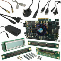
KIT DEVELOPMENT STRATIX IV
Manufacturer
Altera
Series
Stratix® IVr
Type
FPGAr
Datasheets
1.EP4SGX110DF29C3N.pdf
(80 pages)
2.EP4SGX110DF29C3N.pdf
(1154 pages)
3.DK-DEV-4SGX230N.pdf
(2 pages)
4.DK-DEV-4SGX530N.pdf
(57 pages)
Specifications of DK-DEV-4SGX230N
Contents
Development Board, Universal Power Supply, Cables and Software
Silicon Manufacturer
Altera
Core Architecture
FPGA
Core Sub-architecture
Stratix
Silicon Core Number
EP4S
Silicon Family Name
Stratix IV GX
Rohs Compliant
Yes
For Use With/related Products
EP4SGX230K
Lead Free Status / RoHS Status
Lead free / RoHS Compliant
Other names
544-2594
Available stocks
Company
Part Number
Manufacturer
Quantity
Price
Company:

Part Number:
DK-DEV-4SGX230N
Manufacturer:
Altera
Quantity:
135


Chapter 2: Transceiver Clocking in Stratix IV Devices
FPGA Fabric PLLs-Transceiver PLLs Cascading
FPGA Fabric PLLs-Transceiver PLLs Cascading
Table 2–5. Allowed Input Reference Clock Frequency for Example 1
February 2011 Altera Corporation
Multiplication
Factor (M)
10
16
20
25
2
4
5
8
Clock Output from Left and Right PLLs in the FPGA Fabric
You can use the synthesized clock output from one of the left or right PLLs to provide
the input reference clock to the CMU PLLs, 6G ATX PLLs, and receiver CDRs.
Stratix IV devices provide a dedicated clock path from the left PLLs (PLL_L1, PLL_L2,
PLL_L3, and PLL_L4) in the FPGA fabric to the PLL cascade network located on the left
side of the device. Stratix IV devices also provide a dedicated clock path from the
right PLLs (PLL_R1, PLL_R2, PLL_R3, and PLL_R4) in the FPGA fabric to the PLL
cascade network located on the right side of the device. The additional clock
multiplication factors available in the left and right PLLs allow more options for
on-board crystal oscillator frequencies.
The CMU PLL synthesizes the input reference clock to generate the high-speed serial
clock used in the transmitter PMA. The receiver CDR synthesizes the input reference
clock in lock-to-reference (LTR) mode to generate the high-speed serial clock.
This high-speed serial clock output from the CMU PLL and the receiver CDR runs at a
frequency that is half the configured data rate. The CMU PLLs and receiver CDRs
only support multiplication factors (M) of 2, 4, 5, 8, 10, 16, 20, and 25. If you use an
on-board crystal oscillator to provide the input reference clock through the dedicated
refclk pins or ITB lines, the allowed crystal frequencies are limited by the CMU PLL
and the receiver CDR multiplication factors. The input reference clock frequencies are
also limited by the allowed phase frequency detector (PFD) frequency range.
Example 1: Channel Configuration with a 4 Gbps Data Rate
Consider a channel configured for a 4 Gbps data rate. The high-speed serial clock
output from the CMU PLL and the receiver CDR must run at 2 Gbps.
the allowed input reference clock frequencies for Example 1.
For a 4 Gbps data rate, the Quartus II software only allows an input reference clock
frequency of 80, 100, 125, 160, 200, 250, 400, and 500 MHz. To overcome this limitation,
Stratix IV devices allow the synthesized clock output from the left and right PLLs in
the FPGA fabric to drive the CMU PLL and receiver CDR input reference clock. The
additional clock multiplication factors available in the left and right PLLs allow more
options for on-board crystal oscillator frequencies.
On-Board Crystal Reference Clock Frequency (MHz)
With /N = 1
1000
500
400
250
200
125
100
80
With /N = 2
2000
1000
800
500
400
250
200
160
Stratix IV Device Handbook Volume 2: Transceivers
No. Violates the PFD frequency limit.
No. Violates the PFD frequency limit.
Yes but only for /N = 1.
Allowed
Yes
Yes
Yes
Yes
Yes
Table 2–5
lists
2–9
Related parts for DK-DEV-4SGX230N
Image
Part Number
Description
Manufacturer
Datasheet
Request
R

Part Number:
Description:
KIT DEV ARRIA II GX FPGA 2AGX125
Manufacturer:
Altera
Datasheet:

Part Number:
Description:
KIT DEV CYCLONE III LS EP3CLS200
Manufacturer:
Altera
Datasheet:

Part Number:
Description:
KIT DEV STRATIX IV FPGA 4SE530
Manufacturer:
Altera
Datasheet:

Part Number:
Description:
KIT DEV FPGA 2AGX260 W/6.375G TX
Manufacturer:
Altera
Datasheet:

Part Number:
Description:
KIT DEV MAX V 5M570Z
Manufacturer:
Altera
Datasheet:

Part Number:
Description:
KIT DEV STRATIX V FPGA 5SGXEA7
Manufacturer:
Altera
Datasheet:

Part Number:
Description:
KIT DEVELOPMENT STRATIX III
Manufacturer:
Altera
Datasheet:

Part Number:
Description:
KIT DEV ARRIA GX 1AGX60N
Manufacturer:
Altera
Datasheet:
Part Number:
Description:
KIT STARTER CYCLONE IV GX
Manufacturer:
Altera
Datasheet:
Part Number:
Description:
KIT DEVELOPMENT STRATIX IV
Manufacturer:
Altera
Datasheet:

Part Number:
Description:
CPLD, EP610 Family, ECMOS Process, 300 Gates, 16 Macro Cells, 16 Reg., 16 User I/Os, 5V Supply, 35 Speed Grade, 24DIP
Manufacturer:
Altera Corporation
Datasheet:
Part Number:
Description:
CPLD, EP610 Family, ECMOS Process, 300 Gates, 16 Macro Cells, 16 Reg., 16 User I/Os, 5V Supply, 15 Speed Grade, 24DIP
Manufacturer:
Altera Corporation
Datasheet: