DK-DEV-4SGX230N Altera, DK-DEV-4SGX230N Datasheet - Page 70
DK-DEV-4SGX230N
Manufacturer Part Number
DK-DEV-4SGX230N
Description
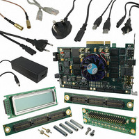
KIT DEVELOPMENT STRATIX IV
Manufacturer
Altera
Series
Stratix® IVr
Type
FPGAr
Datasheets
1.EP4SGX110DF29C3N.pdf
(80 pages)
2.EP4SGX110DF29C3N.pdf
(1154 pages)
3.DK-DEV-4SGX230N.pdf
(2 pages)
4.DK-DEV-4SGX530N.pdf
(57 pages)
Specifications of DK-DEV-4SGX230N
Contents
Development Board, Universal Power Supply, Cables and Software
Silicon Manufacturer
Altera
Core Architecture
FPGA
Core Sub-architecture
Stratix
Silicon Core Number
EP4S
Silicon Family Name
Stratix IV GX
Rohs Compliant
Yes
For Use With/related Products
EP4SGX230K
Lead Free Status / RoHS Status
Lead free / RoHS Compliant
Other names
544-2594
Available stocks
Company
Part Number
Manufacturer
Quantity
Price
Company:

Part Number:
DK-DEV-4SGX230N
Manufacturer:
Altera
Quantity:
135


3–14
Figure 3–13. True Dual-Port Timing Waveform
Stratix IV Device Handbook Volume 1
q_a (asynch)
q_b (asynch)
address_a
address_b
data_a
wren_a
wren_b
clk_a
clk_b
din-1
an-1
doutn-1
Table 3–8
dual-port mode.
Table 3–8. M144K Block Mixed-Width Configurations (True Dual-Port Mode)
In true dual-port mode, M9K and M144K blocks support separate write-enable and
read-enable signals. You can save power by keeping the read-enable signal low
(inactive) when not reading. Read-during-write operations to the same address can
either output “new data” at that location or “old data”. To choose the desired
behavior, set the read-during-write behavior to either new data or old data in the
RAM MegaWizard Plug-In Manager in the Quartus II software. For more information,
refer to
In true dual-port mode, you can access any memory location at any time from either
port. When accessing the same memory location from both ports, you must avoid
possible write conflicts. A write conflict happens when you attempt to write to the
same address location from both ports at the same time. This results in unknown data
being stored to that address location. No conflict resolution circuitry is built into the
Stratix IV TriMatrix memory blocks. You must handle address conflicts external to the
RAM block.
Figure 3–13
and the read operation at port B, with the read-during-write behavior set to new data.
Registering the RAM’s outputs simply delays the q outputs by one clock cycle.
16K × 8
8K × 16
4K × 32
16K × 9
8K × 18
4K × 36
bn
din-1
Read Port
“Read-During-Write Behavior” on page
din
an
lists the possible M144K block mixed-port width configurations in true
shows true dual-port timing waveforms for the write operation at port A
doutn
din
b0
a0
16K × 8
dout0
v
v
v
—
—
—
a1
dout0
dout1
Chapter 3: TriMatrix Embedded Memory Blocks in Stratix IV Devices
8K × 16
b1
v
v
v
—
—
—
a2
dout2
4K × 32
a3
v
v
v
—
—
—
3–18.
Write Port
dout3
dout1
b2
din4
a4
16K × 9
—
—
—
v
v
v
February 2011 Altera Corporation
din4
din5
a5
8K × 18
v
v
v
—
—
—
dout2
din5
b3
din6
a6
Memory Modes
4K × 36
v
v
v
—
—
—
Related parts for DK-DEV-4SGX230N
Image
Part Number
Description
Manufacturer
Datasheet
Request
R

Part Number:
Description:
KIT DEV ARRIA II GX FPGA 2AGX125
Manufacturer:
Altera
Datasheet:

Part Number:
Description:
KIT DEV CYCLONE III LS EP3CLS200
Manufacturer:
Altera
Datasheet:

Part Number:
Description:
KIT DEV STRATIX IV FPGA 4SE530
Manufacturer:
Altera
Datasheet:

Part Number:
Description:
KIT DEV FPGA 2AGX260 W/6.375G TX
Manufacturer:
Altera
Datasheet:

Part Number:
Description:
KIT DEV MAX V 5M570Z
Manufacturer:
Altera
Datasheet:

Part Number:
Description:
KIT DEV STRATIX V FPGA 5SGXEA7
Manufacturer:
Altera
Datasheet:

Part Number:
Description:
KIT DEVELOPMENT STRATIX III
Manufacturer:
Altera
Datasheet:

Part Number:
Description:
KIT DEV ARRIA GX 1AGX60N
Manufacturer:
Altera
Datasheet:
Part Number:
Description:
KIT STARTER CYCLONE IV GX
Manufacturer:
Altera
Datasheet:
Part Number:
Description:
KIT DEVELOPMENT STRATIX IV
Manufacturer:
Altera
Datasheet:

Part Number:
Description:
CPLD, EP610 Family, ECMOS Process, 300 Gates, 16 Macro Cells, 16 Reg., 16 User I/Os, 5V Supply, 35 Speed Grade, 24DIP
Manufacturer:
Altera Corporation
Datasheet:
Part Number:
Description:
CPLD, EP610 Family, ECMOS Process, 300 Gates, 16 Macro Cells, 16 Reg., 16 User I/Os, 5V Supply, 15 Speed Grade, 24DIP
Manufacturer:
Altera Corporation
Datasheet: