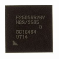
DF2505BR26DV Renesas Electronics America, DF2505BR26DV Datasheet - Page 173

DF2505BR26DV
Manufacturer Part Number
DF2505BR26DV
Description
IC H8S/2505 MCU FLASH 176-LFBGA
Manufacturer
Renesas Electronics America
Series
H8® H8S/2500r
Specifications of DF2505BR26DV
Core Processor
H8S/2000
Core Size
16-Bit
Speed
26MHz
Connectivity
I²C, SCI
Peripherals
POR, PWM, WDT
Number Of I /o
104
Program Memory Size
384KB (384K x 8)
Program Memory Type
FLASH
Ram Size
32K x 8
Voltage - Supply (vcc/vdd)
3 V ~ 5.5 V
Data Converters
A/D 16x10b; D/A 2x8b
Oscillator Type
Internal
Operating Temperature
-40°C ~ 85°C
Package / Case
176-LFBGA
Lead Free Status / RoHS Status
Lead free / RoHS Compliant
Eeprom Size
-
Available stocks
Company
Part Number
Manufacturer
Quantity
Price
Company:
Part Number:
DF2505BR26DV
Manufacturer:
Renesas Electronics America
Quantity:
10 000
- Current page: 173 of 980
- Download datasheet (6Mb)
7.2
Table 7.1 summarizes the pins of the bus controller.
Table 7.1
Note:
7.3
The bus controller has the following registers.
• Bus width control register (ABWCR)
• Access state control register (ASTCR)
• Wait control register H (WCRH)
• Wait control register L (WCRL)
• Bus control register H (BCRH)
• Bus control register L (BCRL)
• Pin function control register (PFCR)
Name
Address strove
Read
High write
Low write
Chip select 0 to 7 CS0 to CS7*
Wait
Bus mastership
request
Bus mastership
request
acknowledge
*
Input/Output Pins
Register Descriptions
CS1 and CS2 are not provided in the H8S/2556 Group.
Pin Configuration
Symbol
AS
RD
HWR
LWR
WAIT
BREQ
BACK
I/O
Output Strobe signal indicating that address output on
Output Strobe signal indicating that external address space is
Output Strobe signal indicating that external address space is
Output Strobe signal indicating that external address space is
Output Strobe signal indicating that areas 0 to 7 are selected.
Input
Input
Output Acknowledge signal indicating that bus has been
Function
address bus is enabled.
being read.
to be written, and upper half (D15 to D8) of data bus is
enabled.
to be written, and lower half (D7 to D0) of data bus is
enabled.
Wait request signal when accessing external 3-state
access space.
Request signal that releases bus to external device.
released.
Rev. 6.00 Sep. 24, 2009 Page 125 of 928
Section 7 Bus Controller
REJ09B0099-0600
Related parts for DF2505BR26DV
Image
Part Number
Description
Manufacturer
Datasheet
Request
R

Part Number:
Description:
KIT STARTER FOR M16C/29
Manufacturer:
Renesas Electronics America
Datasheet:

Part Number:
Description:
KIT STARTER FOR R8C/2D
Manufacturer:
Renesas Electronics America
Datasheet:

Part Number:
Description:
R0K33062P STARTER KIT
Manufacturer:
Renesas Electronics America
Datasheet:

Part Number:
Description:
KIT STARTER FOR R8C/23 E8A
Manufacturer:
Renesas Electronics America
Datasheet:

Part Number:
Description:
KIT STARTER FOR R8C/25
Manufacturer:
Renesas Electronics America
Datasheet:

Part Number:
Description:
KIT STARTER H8S2456 SHARPE DSPLY
Manufacturer:
Renesas Electronics America
Datasheet:

Part Number:
Description:
KIT STARTER FOR R8C38C
Manufacturer:
Renesas Electronics America
Datasheet:

Part Number:
Description:
KIT STARTER FOR R8C35C
Manufacturer:
Renesas Electronics America
Datasheet:

Part Number:
Description:
KIT STARTER FOR R8CL3AC+LCD APPS
Manufacturer:
Renesas Electronics America
Datasheet:

Part Number:
Description:
KIT STARTER FOR RX610
Manufacturer:
Renesas Electronics America
Datasheet:

Part Number:
Description:
KIT STARTER FOR R32C/118
Manufacturer:
Renesas Electronics America
Datasheet:

Part Number:
Description:
KIT DEV RSK-R8C/26-29
Manufacturer:
Renesas Electronics America
Datasheet:

Part Number:
Description:
KIT STARTER FOR SH7124
Manufacturer:
Renesas Electronics America
Datasheet:

Part Number:
Description:
KIT STARTER FOR H8SX/1622
Manufacturer:
Renesas Electronics America
Datasheet:

Part Number:
Description:
KIT DEV FOR SH7203
Manufacturer:
Renesas Electronics America
Datasheet:


