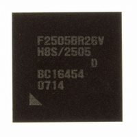
DF2505BR26DV Renesas Electronics America, DF2505BR26DV Datasheet - Page 34

DF2505BR26DV
Manufacturer Part Number
DF2505BR26DV
Description
IC H8S/2505 MCU FLASH 176-LFBGA
Manufacturer
Renesas Electronics America
Series
H8® H8S/2500r
Specifications of DF2505BR26DV
Core Processor
H8S/2000
Core Size
16-Bit
Speed
26MHz
Connectivity
I²C, SCI
Peripherals
POR, PWM, WDT
Number Of I /o
104
Program Memory Size
384KB (384K x 8)
Program Memory Type
FLASH
Ram Size
32K x 8
Voltage - Supply (vcc/vdd)
3 V ~ 5.5 V
Data Converters
A/D 16x10b; D/A 2x8b
Oscillator Type
Internal
Operating Temperature
-40°C ~ 85°C
Package / Case
176-LFBGA
Lead Free Status / RoHS Status
Lead free / RoHS Compliant
Eeprom Size
-
Available stocks
Company
Part Number
Manufacturer
Quantity
Price
Company:
Part Number:
DF2505BR26DV
Manufacturer:
Renesas Electronics America
Quantity:
10 000
- Current page: 34 of 980
- Download datasheet (6Mb)
Figure 10.16 Example of Buffer Operation (2) ............................................................................ 318
Figure 10.17 Cascaded Operation Setting Procedure ................................................................... 319
Figure 10.18 Example of Cascaded Operation (1) ....................................................................... 319
Figure 10.19 Example of Cascaded Operation (2) ....................................................................... 320
Figure 10.20 Example of PWM Mode Setting Procedure ............................................................ 322
Figure 10.21 Example of PWM Mode Operation (1)................................................................... 323
Figure 10.22 Example of PWM Mode Operation (2)................................................................... 323
Figure 10.23 Example of PWM Mode Operation (3)................................................................... 324
Figure 10.24 Example of Phase Counting Mode Setting Procedure ............................................ 326
Figure 10.25 Example of Phase Counting Mode 1 Operation ...................................................... 327
Figure 10.26 Example of Phase Counting Mode 2 Operation ...................................................... 328
Figure 10.27 Example of Phase Counting Mode 3 Operation ...................................................... 329
Figure 10.28 Example of Phase Counting Mode 4 Operation ...................................................... 330
Figure 10.29 Phase Counting Mode Application Example .......................................................... 332
Figure 10.30 Count Timing in Internal Clock Operation ............................................................. 335
Figure 10.31 Count Timing in External Clock Operation ............................................................ 335
Figure 10.32 Output Compare Output Timing ............................................................................. 336
Figure 10.33 Input Capture Input Signal Timing ......................................................................... 336
Figure 10.34 Counter Clear Timing (Compare Match) ................................................................ 337
Figure 10.35 Counter Clear Timing (Input Capture).................................................................... 337
Figure 10.36 Buffer Operation Timing (Compare Match) ........................................................... 338
Figure 10.37 Buffer Operation Timing (Input Capture) ............................................................... 338
Figure 10.38 TGI Interrupt Timing (Compare Match) ................................................................. 339
Figure 10.39 TGI Interrupt Timing (Input Capture)..................................................................... 340
Figure 10.40 TCIV Interrupt Setting Timing ............................................................................... 340
Figure 10.41 TCIU Interrupt Setting Timing ............................................................................... 341
Figure 10.42 Timing for Status Flag Clearing by CPU ................................................................ 342
Figure 10.43 Timing for Status Flag Clearing by DTC Activation .............................................. 342
Figure 10.44 Phase Difference, Overlap, and Pulse Width in Phase Counting Mode .................. 343
Figure 10.45 Contention between TCNT Write and Clear Operations......................................... 344
Figure 10.46 Contention between TCNT Write and Increment Operations ................................. 345
Figure 10.47 Contention between TGR Write and Compare Match ............................................ 346
Figure 10.48 Contention between Buffer Register Write and Compare Match............................ 347
Figure 10.49 Contention between TGR Read and Input Capture ................................................. 348
Figure 10.50 Contention between TGR Write and Input Capture ................................................ 349
Figure 10.51 Contention between Buffer Register Write and Input Capture ............................... 350
Figure 10.52 Contention between Overflow and Counter Clearing ............................................. 351
Figure 10.53 Contention between TCNT Write and Overflow .................................................... 352
Rev. 6.00 Sep. 24, 2009 Page xxxii of xlvi
REJ09B0099-0600
Related parts for DF2505BR26DV
Image
Part Number
Description
Manufacturer
Datasheet
Request
R

Part Number:
Description:
KIT STARTER FOR M16C/29
Manufacturer:
Renesas Electronics America
Datasheet:

Part Number:
Description:
KIT STARTER FOR R8C/2D
Manufacturer:
Renesas Electronics America
Datasheet:

Part Number:
Description:
R0K33062P STARTER KIT
Manufacturer:
Renesas Electronics America
Datasheet:

Part Number:
Description:
KIT STARTER FOR R8C/23 E8A
Manufacturer:
Renesas Electronics America
Datasheet:

Part Number:
Description:
KIT STARTER FOR R8C/25
Manufacturer:
Renesas Electronics America
Datasheet:

Part Number:
Description:
KIT STARTER H8S2456 SHARPE DSPLY
Manufacturer:
Renesas Electronics America
Datasheet:

Part Number:
Description:
KIT STARTER FOR R8C38C
Manufacturer:
Renesas Electronics America
Datasheet:

Part Number:
Description:
KIT STARTER FOR R8C35C
Manufacturer:
Renesas Electronics America
Datasheet:

Part Number:
Description:
KIT STARTER FOR R8CL3AC+LCD APPS
Manufacturer:
Renesas Electronics America
Datasheet:

Part Number:
Description:
KIT STARTER FOR RX610
Manufacturer:
Renesas Electronics America
Datasheet:

Part Number:
Description:
KIT STARTER FOR R32C/118
Manufacturer:
Renesas Electronics America
Datasheet:

Part Number:
Description:
KIT DEV RSK-R8C/26-29
Manufacturer:
Renesas Electronics America
Datasheet:

Part Number:
Description:
KIT STARTER FOR SH7124
Manufacturer:
Renesas Electronics America
Datasheet:

Part Number:
Description:
KIT STARTER FOR H8SX/1622
Manufacturer:
Renesas Electronics America
Datasheet:

Part Number:
Description:
KIT DEV FOR SH7203
Manufacturer:
Renesas Electronics America
Datasheet:


