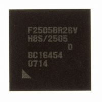
DF2505BR26DV Renesas Electronics America, DF2505BR26DV Datasheet - Page 33

DF2505BR26DV
Manufacturer Part Number
DF2505BR26DV
Description
IC H8S/2505 MCU FLASH 176-LFBGA
Manufacturer
Renesas Electronics America
Series
H8® H8S/2500r
Specifications of DF2505BR26DV
Core Processor
H8S/2000
Core Size
16-Bit
Speed
26MHz
Connectivity
I²C, SCI
Peripherals
POR, PWM, WDT
Number Of I /o
104
Program Memory Size
384KB (384K x 8)
Program Memory Type
FLASH
Ram Size
32K x 8
Voltage - Supply (vcc/vdd)
3 V ~ 5.5 V
Data Converters
A/D 16x10b; D/A 2x8b
Oscillator Type
Internal
Operating Temperature
-40°C ~ 85°C
Package / Case
176-LFBGA
Lead Free Status / RoHS Status
Lead free / RoHS Compliant
Eeprom Size
-
Available stocks
Company
Part Number
Manufacturer
Quantity
Price
Company:
Part Number:
DF2505BR26DV
Manufacturer:
Renesas Electronics America
Quantity:
10 000
- Current page: 33 of 980
- Download datasheet (6Mb)
Figure 7.25 Example of Burst ROM Access Timing (When AST0 = BRSTS1 = 1).................. 158
Figure 7.26 Example of Burst ROM Access Timing (When AST0 = BRSTS1 = 0).................. 158
Figure 7.27 Example of Idle Cycle Operation (1) ...................................................................... 160
Figure 7.28 Example of Idle Cycle Operation (2) ...................................................................... 161
Figure 7.29 Relationship between Chip Select (CS) and Read (RD) ......................................... 162
Figure 7.30 Bus Mastership Released State Transition Timing.................................................. 164
Section 8 Data Transfer Controller (DTC)
Figure 8.1
Figure 8.2
Figure 8.3
Figure 8.4
Figure 8.5
Figure 8.6
Figure 8.7
Figure 8.8
Figure 8.9
Figure 8.10 DTC Operation Timing (Example in Normal Mode or Repeat Mode) ................... 186
Figure 8.11 DTC Operation Timing (Example in Block Transfer Mode, with Block Size of 2)187
Figure 8.12 DTC Operation Timing (Example of Chain Transfer) ............................................ 187
Section 9 I/O Ports
Figure 9.1
Section 10 16-Bit Timer Pulse Unit (TPU)
Figure 10.1 Block Diagram of TPU ........................................................................................... 270
Figure 10.2 Example of Counter Operation Setting Procedure .................................................. 307
Figure 10.3 Free-Running Counter Operation............................................................................ 308
Figure 10.4 Periodic Counter Operation..................................................................................... 309
Figure 10.5 Example of Setting Procedure for Waveform Output by Compare Match.............. 310
Figure 10.6 Example of 0 Output/1 Output Operation ............................................................... 311
Figure 10.7 Example of Toggle Output Operation ..................................................................... 311
Figure 10.8 Example of Input Capture Operation Setting Procedure ......................................... 312
Figure 10.9 Example of Input Capture Operation ...................................................................... 313
Figure 10.10 Example of Synchronous Operation Setting Procedure .......................................... 314
Figure 10.11 Example of Synchronous Operation........................................................................ 315
Figure 10.12 Compare Match Buffer Operation........................................................................... 316
Figure 10.13 Input Capture Buffer Operation .............................................................................. 316
Figure 10.14 Example of Buffer Operation Setting Procedure..................................................... 316
Figure 10.15 Example of Buffer Operation (1) ............................................................................ 317
Flowchart of DTC Operation .................................................................................. 181
Memory Mapping in Normal Mode ........................................................................ 182
Memory Mapping in Repeat Mode ......................................................................... 183
Block Diagram of DTC ........................................................................................... 168
Block Diagram of DTC Activation Source Control ................................................ 175
Location of DTC Register Information in Address Space....................................... 176
Correspondence between DTC Vector Address and Register Information ............. 177
Memory Mapping in Block Transfer Mode ............................................................ 184
Chain Transfer Operation........................................................................................ 185
Types of Open Drain Outputs ................................................................................. 212
Rev. 6.00 Sep. 24, 2009 Page xxxi of xlvi
REJ09B0099-0600
Related parts for DF2505BR26DV
Image
Part Number
Description
Manufacturer
Datasheet
Request
R

Part Number:
Description:
KIT STARTER FOR M16C/29
Manufacturer:
Renesas Electronics America
Datasheet:

Part Number:
Description:
KIT STARTER FOR R8C/2D
Manufacturer:
Renesas Electronics America
Datasheet:

Part Number:
Description:
R0K33062P STARTER KIT
Manufacturer:
Renesas Electronics America
Datasheet:

Part Number:
Description:
KIT STARTER FOR R8C/23 E8A
Manufacturer:
Renesas Electronics America
Datasheet:

Part Number:
Description:
KIT STARTER FOR R8C/25
Manufacturer:
Renesas Electronics America
Datasheet:

Part Number:
Description:
KIT STARTER H8S2456 SHARPE DSPLY
Manufacturer:
Renesas Electronics America
Datasheet:

Part Number:
Description:
KIT STARTER FOR R8C38C
Manufacturer:
Renesas Electronics America
Datasheet:

Part Number:
Description:
KIT STARTER FOR R8C35C
Manufacturer:
Renesas Electronics America
Datasheet:

Part Number:
Description:
KIT STARTER FOR R8CL3AC+LCD APPS
Manufacturer:
Renesas Electronics America
Datasheet:

Part Number:
Description:
KIT STARTER FOR RX610
Manufacturer:
Renesas Electronics America
Datasheet:

Part Number:
Description:
KIT STARTER FOR R32C/118
Manufacturer:
Renesas Electronics America
Datasheet:

Part Number:
Description:
KIT DEV RSK-R8C/26-29
Manufacturer:
Renesas Electronics America
Datasheet:

Part Number:
Description:
KIT STARTER FOR SH7124
Manufacturer:
Renesas Electronics America
Datasheet:

Part Number:
Description:
KIT STARTER FOR H8SX/1622
Manufacturer:
Renesas Electronics America
Datasheet:

Part Number:
Description:
KIT DEV FOR SH7203
Manufacturer:
Renesas Electronics America
Datasheet:


