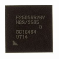
DF2505BR26DV Renesas Electronics America, DF2505BR26DV Datasheet - Page 693

DF2505BR26DV
Manufacturer Part Number
DF2505BR26DV
Description
IC H8S/2505 MCU FLASH 176-LFBGA
Manufacturer
Renesas Electronics America
Series
H8® H8S/2500r
Specifications of DF2505BR26DV
Core Processor
H8S/2000
Core Size
16-Bit
Speed
26MHz
Connectivity
I²C, SCI
Peripherals
POR, PWM, WDT
Number Of I /o
104
Program Memory Size
384KB (384K x 8)
Program Memory Type
FLASH
Ram Size
32K x 8
Voltage - Supply (vcc/vdd)
3 V ~ 5.5 V
Data Converters
A/D 16x10b; D/A 2x8b
Oscillator Type
Internal
Operating Temperature
-40°C ~ 85°C
Package / Case
176-LFBGA
Lead Free Status / RoHS Status
Lead free / RoHS Compliant
Eeprom Size
-
Available stocks
Company
Part Number
Manufacturer
Quantity
Price
Company:
Part Number:
DF2505BR26DV
Manufacturer:
Renesas Electronics America
Quantity:
10 000
- Current page: 693 of 980
- Download datasheet (6Mb)
Section 18 Controller Area Network (HCAN) [H8S/2556 Group]
mailbox interrupt mask register (MBIMR). Interrupt sources of the interrupt register (IRR) can be
masked by IMR.
Arbitration Field Setting: The arbitration field is set by message control registers MCx[5] to
MCx[8] in a transmit mailbox. For a standard format, an 11-bit identifier (ID-28 to ID-18) and the
RTR bit are set, and the IDE bit is cleared to 0. For an extended format, a 29-bit identifier (ID-28
to ID-0) and the RTR bit are set, and the IDE bit is set to 1.
Control Field Setting: In the control field, the byte length of the data to be transmitted is set
within the range of zero to eight bytes. The register to be set is the message control register
MCx[1] in a transmit mailbox.
Data Field Setting: In the data field, the data to be transmitted is set within the range zero to
eight. The registers to be set are the message data registers MDx[1] to MDx[8]. The byte length of
the data to be transmitted is determined by the data length code in the control field. Even if data
exceeding the value set in the control field is set in the data field, up to the byte length set in the
control field will actually be transmitted.
Message Transmission: If the corresponding mailbox transmit wait bit (TXPR1 to TXPR15) in
the transmit wait register (TXPR) is set to 1 after message control and message data registers have
been set, the message enters transmit wait state. If the message is transmitted error-free, the
corresponding acknowledge bit (TXACK1 to TXACK15) in the transmit acknowledge register
(TXACK) is set to 1, and the corresponding transmit wait bit (TXPR1 to TXPR15) in the transmit
wait register (TXPR) is automatically cleared to 0. Also, if the corresponding bit (MBIMR1 to
MBIMR15) in the mailbox interrupt mask register (MBIMR) and the mailbox empty interrupt bit
(IRR8) in the interrupt mask register (IMR) are both simultaneously set to enable interrupts,
interrupts may be sent to the CPU.
If transmission of a transmit message is aborted in the following cases, the message is
retransmitted automatically:
• CAN bus arbitration failure (failure to acquire the bus)
• Error during transmission (bit error, stuff error, CRC error, frame error, or ACK error)
Message Transmission Cancellation: Transmission cancellation can be specified for a message
stored in a mailbox as a transmit wait message. A transmit wait message is canceled by setting the
bit for the corresponding mailbox (TXCR1 to TXCR15) to 1 in the transmit cancel register
(TXCR). Clearing the transmit wait register (TXPR) does not cancel transmission. When
cancellation is executed, the transmit wait register (TXPR) is automatically reset, and the
corresponding bit is set to 1 in the abort acknowledge register (ABACK). An interrupt to the CPU
can be requested, and if the mailbox empty interrupt (IRR8) is enabled for the bits (MBIMR1 to
Rev. 6.00 Sep. 24, 2009 Page 645 of 928
REJ09B0099-0600
Related parts for DF2505BR26DV
Image
Part Number
Description
Manufacturer
Datasheet
Request
R

Part Number:
Description:
KIT STARTER FOR M16C/29
Manufacturer:
Renesas Electronics America
Datasheet:

Part Number:
Description:
KIT STARTER FOR R8C/2D
Manufacturer:
Renesas Electronics America
Datasheet:

Part Number:
Description:
R0K33062P STARTER KIT
Manufacturer:
Renesas Electronics America
Datasheet:

Part Number:
Description:
KIT STARTER FOR R8C/23 E8A
Manufacturer:
Renesas Electronics America
Datasheet:

Part Number:
Description:
KIT STARTER FOR R8C/25
Manufacturer:
Renesas Electronics America
Datasheet:

Part Number:
Description:
KIT STARTER H8S2456 SHARPE DSPLY
Manufacturer:
Renesas Electronics America
Datasheet:

Part Number:
Description:
KIT STARTER FOR R8C38C
Manufacturer:
Renesas Electronics America
Datasheet:

Part Number:
Description:
KIT STARTER FOR R8C35C
Manufacturer:
Renesas Electronics America
Datasheet:

Part Number:
Description:
KIT STARTER FOR R8CL3AC+LCD APPS
Manufacturer:
Renesas Electronics America
Datasheet:

Part Number:
Description:
KIT STARTER FOR RX610
Manufacturer:
Renesas Electronics America
Datasheet:

Part Number:
Description:
KIT STARTER FOR R32C/118
Manufacturer:
Renesas Electronics America
Datasheet:

Part Number:
Description:
KIT DEV RSK-R8C/26-29
Manufacturer:
Renesas Electronics America
Datasheet:

Part Number:
Description:
KIT STARTER FOR SH7124
Manufacturer:
Renesas Electronics America
Datasheet:

Part Number:
Description:
KIT STARTER FOR H8SX/1622
Manufacturer:
Renesas Electronics America
Datasheet:

Part Number:
Description:
KIT DEV FOR SH7203
Manufacturer:
Renesas Electronics America
Datasheet:


