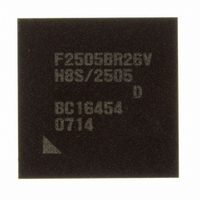
DF2505BR26DV Renesas Electronics America, DF2505BR26DV Datasheet - Page 930

DF2505BR26DV
Manufacturer Part Number
DF2505BR26DV
Description
IC H8S/2505 MCU FLASH 176-LFBGA
Manufacturer
Renesas Electronics America
Series
H8® H8S/2500r
Specifications of DF2505BR26DV
Core Processor
H8S/2000
Core Size
16-Bit
Speed
26MHz
Connectivity
I²C, SCI
Peripherals
POR, PWM, WDT
Number Of I /o
104
Program Memory Size
384KB (384K x 8)
Program Memory Type
FLASH
Ram Size
32K x 8
Voltage - Supply (vcc/vdd)
3 V ~ 5.5 V
Data Converters
A/D 16x10b; D/A 2x8b
Oscillator Type
Internal
Operating Temperature
-40°C ~ 85°C
Package / Case
176-LFBGA
Lead Free Status / RoHS Status
Lead free / RoHS Compliant
Eeprom Size
-
Available stocks
Company
Part Number
Manufacturer
Quantity
Price
Company:
Part Number:
DF2505BR26DV
Manufacturer:
Renesas Electronics America
Quantity:
10 000
- Current page: 930 of 980
- Download datasheet (6Mb)
Section 24 Electrical Characteristics
24.4
Figure 24.2 shows the test conditions for the AC characteristics.
24.4.1
Table 24.5 Power-On/Off Timing
Condition A: V
AV
T
Note:
Rev. 6.00 Sep. 24, 2009 Page 882 of 928
REJ09B0099-0600
Item
Time taken to switch V
on
V
switched off
V
V
a
CC
CC
CC
= –20°C to +75°C (regular specifications)*, T
CC
start voltage
hold time when PV
rising gradient
= 3.0 V to 5.5 V, V
*
AC Characteristics
Power-On/Off Timing
The regular specifications are supported in the H8S/2506 Group only.
LSI output pin
CC
= 3.0 V to 5.5 V, P1V
CC
CC
ref
is
C
= 3.0 V to AV
Symbol
t
t
V
SV
VCCS
VCCH
CCSTART
CC
Figure 24.2 Output Load Circuit
R
H
CC
Min.
−1
−1
⎯
⎯
CC
= 3.0 V to 5.5 V, P2V
, V
5 V
SS
= AV
a
R
= –40°C to +85°C (wide-range specifications)
L
Typ.
⎯
⎯
0
⎯
C = 30 pF
R
R
Input/output timing measurement levels
• Low level: 0.8 V
• High level: 2.0 V
SS
L
H
= 2.4 kΩ
= 12 kΩ
= 0 V,
Max.
—
—
0.8
20
CC
= 3.0 V to 5.5 V,
Unit
ms
ms
V
ms/V
Test Conditions
Figure 24.3
Figure 24.4
Related parts for DF2505BR26DV
Image
Part Number
Description
Manufacturer
Datasheet
Request
R

Part Number:
Description:
KIT STARTER FOR M16C/29
Manufacturer:
Renesas Electronics America
Datasheet:

Part Number:
Description:
KIT STARTER FOR R8C/2D
Manufacturer:
Renesas Electronics America
Datasheet:

Part Number:
Description:
R0K33062P STARTER KIT
Manufacturer:
Renesas Electronics America
Datasheet:

Part Number:
Description:
KIT STARTER FOR R8C/23 E8A
Manufacturer:
Renesas Electronics America
Datasheet:

Part Number:
Description:
KIT STARTER FOR R8C/25
Manufacturer:
Renesas Electronics America
Datasheet:

Part Number:
Description:
KIT STARTER H8S2456 SHARPE DSPLY
Manufacturer:
Renesas Electronics America
Datasheet:

Part Number:
Description:
KIT STARTER FOR R8C38C
Manufacturer:
Renesas Electronics America
Datasheet:

Part Number:
Description:
KIT STARTER FOR R8C35C
Manufacturer:
Renesas Electronics America
Datasheet:

Part Number:
Description:
KIT STARTER FOR R8CL3AC+LCD APPS
Manufacturer:
Renesas Electronics America
Datasheet:

Part Number:
Description:
KIT STARTER FOR RX610
Manufacturer:
Renesas Electronics America
Datasheet:

Part Number:
Description:
KIT STARTER FOR R32C/118
Manufacturer:
Renesas Electronics America
Datasheet:

Part Number:
Description:
KIT DEV RSK-R8C/26-29
Manufacturer:
Renesas Electronics America
Datasheet:

Part Number:
Description:
KIT STARTER FOR SH7124
Manufacturer:
Renesas Electronics America
Datasheet:

Part Number:
Description:
KIT STARTER FOR H8SX/1622
Manufacturer:
Renesas Electronics America
Datasheet:

Part Number:
Description:
KIT DEV FOR SH7203
Manufacturer:
Renesas Electronics America
Datasheet:


