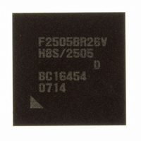
DF2505BR26DV Renesas Electronics America, DF2505BR26DV Datasheet - Page 490

DF2505BR26DV
Manufacturer Part Number
DF2505BR26DV
Description
IC H8S/2505 MCU FLASH 176-LFBGA
Manufacturer
Renesas Electronics America
Series
H8® H8S/2500r
Specifications of DF2505BR26DV
Core Processor
H8S/2000
Core Size
16-Bit
Speed
26MHz
Connectivity
I²C, SCI
Peripherals
POR, PWM, WDT
Number Of I /o
104
Program Memory Size
384KB (384K x 8)
Program Memory Type
FLASH
Ram Size
32K x 8
Voltage - Supply (vcc/vdd)
3 V ~ 5.5 V
Data Converters
A/D 16x10b; D/A 2x8b
Oscillator Type
Internal
Operating Temperature
-40°C ~ 85°C
Package / Case
176-LFBGA
Lead Free Status / RoHS Status
Lead free / RoHS Compliant
Eeprom Size
-
Available stocks
Company
Part Number
Manufacturer
Quantity
Price
Company:
Part Number:
DF2505BR26DV
Manufacturer:
Renesas Electronics America
Quantity:
10 000
- Current page: 490 of 980
- Download datasheet (6Mb)
Section 13 Serial Communication Interface (SCI)
Rev. 6.00 Sep. 24, 2009 Page 442 of 928
REJ09B0099-0600
No
No
No
Figure 13.13 Sample Multiprocessor Serial Reception Flowchart (1)
Read ORER and FER flags in SSR
Read ORER and FER flags in SSR
Read receive data in RDR
Read receive data in RDR
Set MPIE bit in SCR to 1
Read RDRF flag in SSR
Read RDRF flag in SSR
Clear RE bit in SCR to 0
All data received?
This station’s ID?
FER ORER = 1
FER ORER = 1
Start reception
Initialization
RDRF = 1
RDRF = 1
<End>
Yes
Yes
Yes
Yes
No
No
Yes
No
Yes
Error processing
[3]
[1]
[2]
(Continued on
next page)
[4]
[5]
[1] SCI initialization:
[2] ID reception cycle:
[3] SCI status check, ID reception and
[4] SCI status check and data reception:
[5] Receive error processing and break
The RxD pin is automatically designated
as the receive data input pin.
Set the MPIE bit in SCR to 1.
comparison:
Read SSR and check that the RDRF
flag is set to 1, then read the receive
data in RDR and compare it with this
station’s ID.
If the data is not this station’s ID, set the
MPIE bit to 1 again, and clear the RDRF
flag to 0.
If the data is this station’s ID, clear the
RDRF flag to 0.
Read SSR and check that the RDRF
flag is set to 1, then read the data in
RDR.
detection:
If a receive error occurs, read the ORER
and FER flags in SSR to identify the
error. After performing the appropriate
error processing, ensure that the ORER
and FER flags are all cleared to 0.
Reception cannot be resumed if either
of these flags is set to 1.
In the case of a framing error, a break
can be detected by reading the RxD pin
value.
Related parts for DF2505BR26DV
Image
Part Number
Description
Manufacturer
Datasheet
Request
R

Part Number:
Description:
KIT STARTER FOR M16C/29
Manufacturer:
Renesas Electronics America
Datasheet:

Part Number:
Description:
KIT STARTER FOR R8C/2D
Manufacturer:
Renesas Electronics America
Datasheet:

Part Number:
Description:
R0K33062P STARTER KIT
Manufacturer:
Renesas Electronics America
Datasheet:

Part Number:
Description:
KIT STARTER FOR R8C/23 E8A
Manufacturer:
Renesas Electronics America
Datasheet:

Part Number:
Description:
KIT STARTER FOR R8C/25
Manufacturer:
Renesas Electronics America
Datasheet:

Part Number:
Description:
KIT STARTER H8S2456 SHARPE DSPLY
Manufacturer:
Renesas Electronics America
Datasheet:

Part Number:
Description:
KIT STARTER FOR R8C38C
Manufacturer:
Renesas Electronics America
Datasheet:

Part Number:
Description:
KIT STARTER FOR R8C35C
Manufacturer:
Renesas Electronics America
Datasheet:

Part Number:
Description:
KIT STARTER FOR R8CL3AC+LCD APPS
Manufacturer:
Renesas Electronics America
Datasheet:

Part Number:
Description:
KIT STARTER FOR RX610
Manufacturer:
Renesas Electronics America
Datasheet:

Part Number:
Description:
KIT STARTER FOR R32C/118
Manufacturer:
Renesas Electronics America
Datasheet:

Part Number:
Description:
KIT DEV RSK-R8C/26-29
Manufacturer:
Renesas Electronics America
Datasheet:

Part Number:
Description:
KIT STARTER FOR SH7124
Manufacturer:
Renesas Electronics America
Datasheet:

Part Number:
Description:
KIT STARTER FOR H8SX/1622
Manufacturer:
Renesas Electronics America
Datasheet:

Part Number:
Description:
KIT DEV FOR SH7203
Manufacturer:
Renesas Electronics America
Datasheet:


