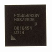
DF2505BR26DV Renesas Electronics America, DF2505BR26DV Datasheet - Page 592

DF2505BR26DV
Manufacturer Part Number
DF2505BR26DV
Description
IC H8S/2505 MCU FLASH 176-LFBGA
Manufacturer
Renesas Electronics America
Series
H8® H8S/2500r
Specifications of DF2505BR26DV
Core Processor
H8S/2000
Core Size
16-Bit
Speed
26MHz
Connectivity
I²C, SCI
Peripherals
POR, PWM, WDT
Number Of I /o
104
Program Memory Size
384KB (384K x 8)
Program Memory Type
FLASH
Ram Size
32K x 8
Voltage - Supply (vcc/vdd)
3 V ~ 5.5 V
Data Converters
A/D 16x10b; D/A 2x8b
Oscillator Type
Internal
Operating Temperature
-40°C ~ 85°C
Package / Case
176-LFBGA
Lead Free Status / RoHS Status
Lead free / RoHS Compliant
Eeprom Size
-
Available stocks
Company
Part Number
Manufacturer
Quantity
Price
Company:
Part Number:
DF2505BR26DV
Manufacturer:
Renesas Electronics America
Quantity:
10 000
- Current page: 592 of 980
- Download datasheet (6Mb)
Section 17 IEBus™ Controller (IEB) [H8S/2552 Group]
(1)
Header is comprised of a start bit and a broadcast bit.
(a) Start Bit
(b) Broadcast Bit
Rev. 6.00 Sep. 24, 2009 Page 544 of 928
REJ09B0099-0600
Note: The value of acknowledge bit is ignored in broadcast communications.
The start bit is a signal for informing a start of data transfer to other units. A unit, which
attempts to start data transfer, outputs a low-level signal (start bit) for a specified period and
then outputs the broadcast bit.
If another unit is already outputting a start bit when a unit attempts to output a start bit, the unit
waits for completion of output of the start bit from the other unit without outputting the start
bit, and then outputs the broadcast bit synchronized with the completion timing.
Other units enter the receive state after detecting the start bit.
The broadcast bit is a bit to identify the type of communications: broadcast or normal.
When this bit is cleared to 0, it indicates the broadcast communications. When it is set to 1, it
indicates the normal communications. Broadcast communications includes group broadcast
and general broadcast, which are identified by a value of the slave address. (For details of the
slave address, see section 17.1.2 (3), Slave Address Field.)
Since there are multiple slave units, which are communications destination units, in the case of
broadcast communications, the acknowledge bit is not returned from each field described in (b)
and below.
Field name
Transfer
Number
Mode 0
Mode 1
Mode 2
Header
of bits
time
Start
P: Parity bit (1 bit)
A: Acknowledge bit (1 bit)
N: Number of bytes
bit
Header
1
When A = 0: ACK
When A = 1: NAK
Broad-
cast
bit
1
address field
address
Master
Master
12
Figure 17.2 Transfer Signal Format
1
P
Approximately 7330 μs
Approximately 2090 μs
Approximately 1590 μs
Slave address
address
Slave
12
field
P A
1
1
Control
Control field
bits
4
P A
1
1
Message
length
length field
8
bits
Message
1
P A
1
Data
(When φ = 12, 18, or 24MHz)
bits
8
Approximately 1590 × N μs
Approximately 410 × N μs
Approximately 300 × N μs
1
P A
Data field
1
Data
bits
8
1
P A
1
Related parts for DF2505BR26DV
Image
Part Number
Description
Manufacturer
Datasheet
Request
R

Part Number:
Description:
KIT STARTER FOR M16C/29
Manufacturer:
Renesas Electronics America
Datasheet:

Part Number:
Description:
KIT STARTER FOR R8C/2D
Manufacturer:
Renesas Electronics America
Datasheet:

Part Number:
Description:
R0K33062P STARTER KIT
Manufacturer:
Renesas Electronics America
Datasheet:

Part Number:
Description:
KIT STARTER FOR R8C/23 E8A
Manufacturer:
Renesas Electronics America
Datasheet:

Part Number:
Description:
KIT STARTER FOR R8C/25
Manufacturer:
Renesas Electronics America
Datasheet:

Part Number:
Description:
KIT STARTER H8S2456 SHARPE DSPLY
Manufacturer:
Renesas Electronics America
Datasheet:

Part Number:
Description:
KIT STARTER FOR R8C38C
Manufacturer:
Renesas Electronics America
Datasheet:

Part Number:
Description:
KIT STARTER FOR R8C35C
Manufacturer:
Renesas Electronics America
Datasheet:

Part Number:
Description:
KIT STARTER FOR R8CL3AC+LCD APPS
Manufacturer:
Renesas Electronics America
Datasheet:

Part Number:
Description:
KIT STARTER FOR RX610
Manufacturer:
Renesas Electronics America
Datasheet:

Part Number:
Description:
KIT STARTER FOR R32C/118
Manufacturer:
Renesas Electronics America
Datasheet:

Part Number:
Description:
KIT DEV RSK-R8C/26-29
Manufacturer:
Renesas Electronics America
Datasheet:

Part Number:
Description:
KIT STARTER FOR SH7124
Manufacturer:
Renesas Electronics America
Datasheet:

Part Number:
Description:
KIT STARTER FOR H8SX/1622
Manufacturer:
Renesas Electronics America
Datasheet:

Part Number:
Description:
KIT DEV FOR SH7203
Manufacturer:
Renesas Electronics America
Datasheet:


