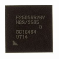
DF2505BR26DV Renesas Electronics America, DF2505BR26DV Datasheet - Page 594

DF2505BR26DV
Manufacturer Part Number
DF2505BR26DV
Description
IC H8S/2505 MCU FLASH 176-LFBGA
Manufacturer
Renesas Electronics America
Series
H8® H8S/2500r
Specifications of DF2505BR26DV
Core Processor
H8S/2000
Core Size
16-Bit
Speed
26MHz
Connectivity
I²C, SCI
Peripherals
POR, PWM, WDT
Number Of I /o
104
Program Memory Size
384KB (384K x 8)
Program Memory Type
FLASH
Ram Size
32K x 8
Voltage - Supply (vcc/vdd)
3 V ~ 5.5 V
Data Converters
A/D 16x10b; D/A 2x8b
Oscillator Type
Internal
Operating Temperature
-40°C ~ 85°C
Package / Case
176-LFBGA
Lead Free Status / RoHS Status
Lead free / RoHS Compliant
Eeprom Size
-
Available stocks
Company
Part Number
Manufacturer
Quantity
Price
Company:
Part Number:
DF2505BR26DV
Manufacturer:
Renesas Electronics America
Quantity:
10 000
- Current page: 594 of 980
- Download datasheet (6Mb)
Section 17 IEBus™ Controller (IEB) [H8S/2552 Group]
The slave unit returns the acknowledgement when the slave addresses match and the parities of the
master and slave addresses are correct. When either of the parities of the master and slave
addresses is wrong, the slave unit decides that the master or slave address is not correctly received
and does not return the acknowledgement. In this case, the master unit enters the waiting (monitor)
state, and communications end.
In the case of broadcast communications, the slave address is used to identify the type of broadcast
communications (group or general) as follows:
• When the slave address is H'FFF: General broadcast communications
• When the slave address is other than H'FFF: Group broadcast communications
Note: The group number is the upper 4-bit value of the slave address in group broadcast
(4)
The control field is a field for transmitting the type and direction of the following data field. The
control field is comprised of control bits, a parity bit, and an acknowledge bit.
The control bits include four bits and are output MSB first.
The parity bit is output following the control bits. When the parity is correct, and the slave unit
can implement the function required from the master unit, the slave unit returns the
acknowledgement and enters the message length field output state. However, if the slave unit
cannot implement the requirements from the master unit even though the parity is correct, or if the
parity is not correct, the slave unit does not return the acknowledgement, and returns to the
waiting (monitor) state.
The master unit enters the subsequent message length field output state after confirming the
acknowledgement.
When the acknowledgement is not confirmed, the master unit enters the waiting (monitor) state,
and communications end. However, in the case of broadcast communications, the master unit
enters the following message length field output state without confirming the acknowledgement.
For details of the contents of the control bit, see table 17.4.
(5)
The message length field is a field for specifying the number of transfer bytes. The message length
field is comprised of message length bits, a parity bit, and an acknowledge bit.
Rev. 6.00 Sep. 24, 2009 Page 546 of 928
REJ09B0099-0600
Control Field
Message Length Field
communications.
Related parts for DF2505BR26DV
Image
Part Number
Description
Manufacturer
Datasheet
Request
R

Part Number:
Description:
KIT STARTER FOR M16C/29
Manufacturer:
Renesas Electronics America
Datasheet:

Part Number:
Description:
KIT STARTER FOR R8C/2D
Manufacturer:
Renesas Electronics America
Datasheet:

Part Number:
Description:
R0K33062P STARTER KIT
Manufacturer:
Renesas Electronics America
Datasheet:

Part Number:
Description:
KIT STARTER FOR R8C/23 E8A
Manufacturer:
Renesas Electronics America
Datasheet:

Part Number:
Description:
KIT STARTER FOR R8C/25
Manufacturer:
Renesas Electronics America
Datasheet:

Part Number:
Description:
KIT STARTER H8S2456 SHARPE DSPLY
Manufacturer:
Renesas Electronics America
Datasheet:

Part Number:
Description:
KIT STARTER FOR R8C38C
Manufacturer:
Renesas Electronics America
Datasheet:

Part Number:
Description:
KIT STARTER FOR R8C35C
Manufacturer:
Renesas Electronics America
Datasheet:

Part Number:
Description:
KIT STARTER FOR R8CL3AC+LCD APPS
Manufacturer:
Renesas Electronics America
Datasheet:

Part Number:
Description:
KIT STARTER FOR RX610
Manufacturer:
Renesas Electronics America
Datasheet:

Part Number:
Description:
KIT STARTER FOR R32C/118
Manufacturer:
Renesas Electronics America
Datasheet:

Part Number:
Description:
KIT DEV RSK-R8C/26-29
Manufacturer:
Renesas Electronics America
Datasheet:

Part Number:
Description:
KIT STARTER FOR SH7124
Manufacturer:
Renesas Electronics America
Datasheet:

Part Number:
Description:
KIT STARTER FOR H8SX/1622
Manufacturer:
Renesas Electronics America
Datasheet:

Part Number:
Description:
KIT DEV FOR SH7203
Manufacturer:
Renesas Electronics America
Datasheet:


