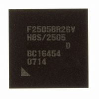
DF2505BR26DV Renesas Electronics America, DF2505BR26DV Datasheet - Page 779

DF2505BR26DV
Manufacturer Part Number
DF2505BR26DV
Description
IC H8S/2505 MCU FLASH 176-LFBGA
Manufacturer
Renesas Electronics America
Series
H8® H8S/2500r
Specifications of DF2505BR26DV
Core Processor
H8S/2000
Core Size
16-Bit
Speed
26MHz
Connectivity
I²C, SCI
Peripherals
POR, PWM, WDT
Number Of I /o
104
Program Memory Size
384KB (384K x 8)
Program Memory Type
FLASH
Ram Size
32K x 8
Voltage - Supply (vcc/vdd)
3 V ~ 5.5 V
Data Converters
A/D 16x10b; D/A 2x8b
Oscillator Type
Internal
Operating Temperature
-40°C ~ 85°C
Package / Case
176-LFBGA
Lead Free Status / RoHS Status
Lead free / RoHS Compliant
Eeprom Size
-
Available stocks
Company
Part Number
Manufacturer
Quantity
Price
Company:
Part Number:
DF2505BR26DV
Manufacturer:
Renesas Electronics America
Quantity:
10 000
- Current page: 779 of 980
- Download datasheet (6Mb)
1. After the data to be programmed has fixed values, clear the RAMS bit to cancel the overlap of
2. Move the fixed programmed data in the overlap area in the RAM to the area to which the
3. Transfer the user-created programming/erasing-procedure program to the RAM.
4. Run the programming/erasing-procedure program on the RAM and download the on-chip
5. When the EB0 area of the user MAT has not been erased, the programming program must be
Note: Setting the RAMS bit to 1 puts all the blocks in the flash MAT into a program/erase-
RAM.
programming/erasing program created by the user is transferred and outside the area in which
on-chip programs are downloaded.
programming/erasing program.
downloaded after erasing. Set the parameters FMPAR and FMPDR in the data to be
programmed so that the tuned data that has been saved is designated, and execute
programming.
protected state regardless of the values of the RAM2 to RAM0 bits (emulation protection).
In this state, downloading of the on-chip programs is also disabled, so clear the RAMS bit
before actual programming or erasure.
Note:
H'7FFFF *
H'00000
H'01000
H'02000
H'03000
H'04000
H'05000
H'06000
H'07000
H'08000
The H8S/2551 and H8S/2505 flash memory user MATs are allocated address
H'00000 to H'5FFFF and divided into EB0 to EB13 erasure blocks.
Figure 20.19 Programming of the Data after Tuning
Flash memory
EB8 to EB15*
(user MAT)
EB0
EB1
EB2
EB3
EB4
EB5
EB6
EB7
(1) Cancel the emulation mode.
(2) Move tuned data from the operlap area to the
(3) Transfer the program/erase-procedure program.
(4) Download the on-chip programming/erasing
(5) Execute programming after erasing,
programs.
as necessary.
area with no programming/erasing data.
programming-procedure
Copy of the tuned data
Download area
On-chip RAM
Area for the
program
Rev. 6.00 Sep. 24, 2009 Page 731 of 928
H'FFC000
H'FFC800
H'FFD000
H'FFDFFF
H'FFEFBF
Section 20 Flash Memory
REJ09B0099-0600
Related parts for DF2505BR26DV
Image
Part Number
Description
Manufacturer
Datasheet
Request
R

Part Number:
Description:
KIT STARTER FOR M16C/29
Manufacturer:
Renesas Electronics America
Datasheet:

Part Number:
Description:
KIT STARTER FOR R8C/2D
Manufacturer:
Renesas Electronics America
Datasheet:

Part Number:
Description:
R0K33062P STARTER KIT
Manufacturer:
Renesas Electronics America
Datasheet:

Part Number:
Description:
KIT STARTER FOR R8C/23 E8A
Manufacturer:
Renesas Electronics America
Datasheet:

Part Number:
Description:
KIT STARTER FOR R8C/25
Manufacturer:
Renesas Electronics America
Datasheet:

Part Number:
Description:
KIT STARTER H8S2456 SHARPE DSPLY
Manufacturer:
Renesas Electronics America
Datasheet:

Part Number:
Description:
KIT STARTER FOR R8C38C
Manufacturer:
Renesas Electronics America
Datasheet:

Part Number:
Description:
KIT STARTER FOR R8C35C
Manufacturer:
Renesas Electronics America
Datasheet:

Part Number:
Description:
KIT STARTER FOR R8CL3AC+LCD APPS
Manufacturer:
Renesas Electronics America
Datasheet:

Part Number:
Description:
KIT STARTER FOR RX610
Manufacturer:
Renesas Electronics America
Datasheet:

Part Number:
Description:
KIT STARTER FOR R32C/118
Manufacturer:
Renesas Electronics America
Datasheet:

Part Number:
Description:
KIT DEV RSK-R8C/26-29
Manufacturer:
Renesas Electronics America
Datasheet:

Part Number:
Description:
KIT STARTER FOR SH7124
Manufacturer:
Renesas Electronics America
Datasheet:

Part Number:
Description:
KIT STARTER FOR H8SX/1622
Manufacturer:
Renesas Electronics America
Datasheet:

Part Number:
Description:
KIT DEV FOR SH7203
Manufacturer:
Renesas Electronics America
Datasheet:


