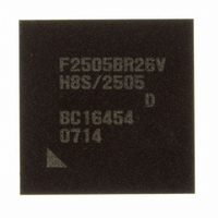
DF2505BR26DV Renesas Electronics America, DF2505BR26DV Datasheet - Page 252

DF2505BR26DV
Manufacturer Part Number
DF2505BR26DV
Description
IC H8S/2505 MCU FLASH 176-LFBGA
Manufacturer
Renesas Electronics America
Series
H8® H8S/2500r
Specifications of DF2505BR26DV
Core Processor
H8S/2000
Core Size
16-Bit
Speed
26MHz
Connectivity
I²C, SCI
Peripherals
POR, PWM, WDT
Number Of I /o
104
Program Memory Size
384KB (384K x 8)
Program Memory Type
FLASH
Ram Size
32K x 8
Voltage - Supply (vcc/vdd)
3 V ~ 5.5 V
Data Converters
A/D 16x10b; D/A 2x8b
Oscillator Type
Internal
Operating Temperature
-40°C ~ 85°C
Package / Case
176-LFBGA
Lead Free Status / RoHS Status
Lead free / RoHS Compliant
Eeprom Size
-
Available stocks
Company
Part Number
Manufacturer
Quantity
Price
Company:
Part Number:
DF2505BR26DV
Manufacturer:
Renesas Electronics America
Quantity:
10 000
- Current page: 252 of 980
- Download datasheet (6Mb)
Section 9 I/O Ports
• P11/TIOCB0
Notes: 1. For the setting of the TPU channel, see section 10, 16-Bit Timer Pulse Unit (TPU).
• P10/TIOCA0
Notes: 1. For the setting of the TPU channel, see section 10, 16-Bit Timer Pulse Unit (TPU).
Rev. 6.00 Sep. 24, 2009 Page 204 of 928
REJ09B0099-0600
TPU Channel 0 Setting*
P11DDR
Pin function
TPU Channel 0 Setting*
P10DDR
Pin function
The pin function is switched as shown below according to the combination of the TPU channel
0 setting and the P11DDR bit.
The pin function is switched as shown below according to the combination of the TPU channel
0 setting and the P10DDR bit.
2. This pin functions as TIOCB0 input when TPU channel 0 timer operating mode is set to
2. This pin functions as TIOCA0 input when TPU channel 0 timer operating mode is set to
normal operation and IOB3 to IOB0 in TIORH_0 are set to 10xx.
normal operation and IOA3 to IOA0 in TIORH_0 are set to 10xx.
1
1
TIOCB0 output
TIOCA0 output
Output
Output
⎯
⎯
P11 input
P10 input
0
0
Input or Initial Value
Input or Initial Value
TIOCB0 input*
TIOCA0 input*
P11 output
P10 output
2
2
1
1
Related parts for DF2505BR26DV
Image
Part Number
Description
Manufacturer
Datasheet
Request
R

Part Number:
Description:
KIT STARTER FOR M16C/29
Manufacturer:
Renesas Electronics America
Datasheet:

Part Number:
Description:
KIT STARTER FOR R8C/2D
Manufacturer:
Renesas Electronics America
Datasheet:

Part Number:
Description:
R0K33062P STARTER KIT
Manufacturer:
Renesas Electronics America
Datasheet:

Part Number:
Description:
KIT STARTER FOR R8C/23 E8A
Manufacturer:
Renesas Electronics America
Datasheet:

Part Number:
Description:
KIT STARTER FOR R8C/25
Manufacturer:
Renesas Electronics America
Datasheet:

Part Number:
Description:
KIT STARTER H8S2456 SHARPE DSPLY
Manufacturer:
Renesas Electronics America
Datasheet:

Part Number:
Description:
KIT STARTER FOR R8C38C
Manufacturer:
Renesas Electronics America
Datasheet:

Part Number:
Description:
KIT STARTER FOR R8C35C
Manufacturer:
Renesas Electronics America
Datasheet:

Part Number:
Description:
KIT STARTER FOR R8CL3AC+LCD APPS
Manufacturer:
Renesas Electronics America
Datasheet:

Part Number:
Description:
KIT STARTER FOR RX610
Manufacturer:
Renesas Electronics America
Datasheet:

Part Number:
Description:
KIT STARTER FOR R32C/118
Manufacturer:
Renesas Electronics America
Datasheet:

Part Number:
Description:
KIT DEV RSK-R8C/26-29
Manufacturer:
Renesas Electronics America
Datasheet:

Part Number:
Description:
KIT STARTER FOR SH7124
Manufacturer:
Renesas Electronics America
Datasheet:

Part Number:
Description:
KIT STARTER FOR H8SX/1622
Manufacturer:
Renesas Electronics America
Datasheet:

Part Number:
Description:
KIT DEV FOR SH7203
Manufacturer:
Renesas Electronics America
Datasheet:


