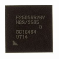
DF2505BR26DV Renesas Electronics America, DF2505BR26DV Datasheet - Page 688

DF2505BR26DV
Manufacturer Part Number
DF2505BR26DV
Description
IC H8S/2505 MCU FLASH 176-LFBGA
Manufacturer
Renesas Electronics America
Series
H8® H8S/2500r
Specifications of DF2505BR26DV
Core Processor
H8S/2000
Core Size
16-Bit
Speed
26MHz
Connectivity
I²C, SCI
Peripherals
POR, PWM, WDT
Number Of I /o
104
Program Memory Size
384KB (384K x 8)
Program Memory Type
FLASH
Ram Size
32K x 8
Voltage - Supply (vcc/vdd)
3 V ~ 5.5 V
Data Converters
A/D 16x10b; D/A 2x8b
Oscillator Type
Internal
Operating Temperature
-40°C ~ 85°C
Package / Case
176-LFBGA
Lead Free Status / RoHS Status
Lead free / RoHS Compliant
Eeprom Size
-
Available stocks
Company
Part Number
Manufacturer
Quantity
Price
Company:
Part Number:
DF2505BR26DV
Manufacturer:
Renesas Electronics America
Quantity:
10 000
- Current page: 688 of 980
- Download datasheet (6Mb)
Section 18 Controller Area Network (HCAN) [H8S/2556 Group]
Bit Rate and Bit Timing Settings: The bit rate and bit timing settings are made in the bit
configuration register (BCR). Settings should be made such that all CAN controllers connected to
the CAN bus have the same baud rate and bit width. The 1-bit time consists of the total of the
settable time quantum (TQ). Though BCR can always be written to, it should not be modified in
other than configuration mode.
SYNC_SEG is a segment for establishing the synchronization of nodes on the CAN bus. Normal
bit edge transitions occur in this segment. PRSEG is a segment for compensating for the physical
delay between networks. PHSEG1 is a buffer segment for correcting phase drift (positive). This
segment is extended when synchronization (resynchronization) is established. PHSEG2 is a buffer
segment for correcting phase drift (negative). This segment is shortened when synchronization
(resynchronization) is established. Limits on the settable value (TSEG1, TSEG2, BRP, BSP, and
SJW) are shown in table 18.2.
Table 18.2 Limits for Settable Value
Notes: 1. SJW is stipulated in the CAN specifications:
Rev. 6.00 Sep. 24, 2009 Page 640 of 928
REJ09B0099-0600
Name
Time segment 1
Time segment 2
Baud rate prescaler
Bit sample point
Re-synchronization jump width
2. The minimum value of TSEG2 is stipulated in the CAN specifications:
3. The minimum value of TSEG1 is stipulated in the CAN specifications:
3 ≥ SJW ≥ 0
TSEG2 ≥ SJW
TSEG1 > TSEG2
1 time quantaum
SYNC_SEG
Figure 18.8 Detailed Description of One Bit
PRSEG
1-bit time (8 to 25 time quanta)
Time segment 1 (TSEG1)
4 to 16 time quanta
Abbreviation
TSEG1
TSEG2
BRP
BSP
SJW*
1
PHSEG1
Min. Value
B'0011*
B'001*
B'000000
B'0
B'00
2 to 8 time quanta
2
Time segment 2
3
(TSEG2)
PHSEG2
Max. Value
B'1111
B'111
B'111111
B'1
B'11
Related parts for DF2505BR26DV
Image
Part Number
Description
Manufacturer
Datasheet
Request
R

Part Number:
Description:
KIT STARTER FOR M16C/29
Manufacturer:
Renesas Electronics America
Datasheet:

Part Number:
Description:
KIT STARTER FOR R8C/2D
Manufacturer:
Renesas Electronics America
Datasheet:

Part Number:
Description:
R0K33062P STARTER KIT
Manufacturer:
Renesas Electronics America
Datasheet:

Part Number:
Description:
KIT STARTER FOR R8C/23 E8A
Manufacturer:
Renesas Electronics America
Datasheet:

Part Number:
Description:
KIT STARTER FOR R8C/25
Manufacturer:
Renesas Electronics America
Datasheet:

Part Number:
Description:
KIT STARTER H8S2456 SHARPE DSPLY
Manufacturer:
Renesas Electronics America
Datasheet:

Part Number:
Description:
KIT STARTER FOR R8C38C
Manufacturer:
Renesas Electronics America
Datasheet:

Part Number:
Description:
KIT STARTER FOR R8C35C
Manufacturer:
Renesas Electronics America
Datasheet:

Part Number:
Description:
KIT STARTER FOR R8CL3AC+LCD APPS
Manufacturer:
Renesas Electronics America
Datasheet:

Part Number:
Description:
KIT STARTER FOR RX610
Manufacturer:
Renesas Electronics America
Datasheet:

Part Number:
Description:
KIT STARTER FOR R32C/118
Manufacturer:
Renesas Electronics America
Datasheet:

Part Number:
Description:
KIT DEV RSK-R8C/26-29
Manufacturer:
Renesas Electronics America
Datasheet:

Part Number:
Description:
KIT STARTER FOR SH7124
Manufacturer:
Renesas Electronics America
Datasheet:

Part Number:
Description:
KIT STARTER FOR H8SX/1622
Manufacturer:
Renesas Electronics America
Datasheet:

Part Number:
Description:
KIT DEV FOR SH7203
Manufacturer:
Renesas Electronics America
Datasheet:


