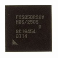
DF2505BR26DV Renesas Electronics America, DF2505BR26DV Datasheet - Page 497

DF2505BR26DV
Manufacturer Part Number
DF2505BR26DV
Description
IC H8S/2505 MCU FLASH 176-LFBGA
Manufacturer
Renesas Electronics America
Series
H8® H8S/2500r
Specifications of DF2505BR26DV
Core Processor
H8S/2000
Core Size
16-Bit
Speed
26MHz
Connectivity
I²C, SCI
Peripherals
POR, PWM, WDT
Number Of I /o
104
Program Memory Size
384KB (384K x 8)
Program Memory Type
FLASH
Ram Size
32K x 8
Voltage - Supply (vcc/vdd)
3 V ~ 5.5 V
Data Converters
A/D 16x10b; D/A 2x8b
Oscillator Type
Internal
Operating Temperature
-40°C ~ 85°C
Package / Case
176-LFBGA
Lead Free Status / RoHS Status
Lead free / RoHS Compliant
Eeprom Size
-
Available stocks
Company
Part Number
Manufacturer
Quantity
Price
Company:
Part Number:
DF2505BR26DV
Manufacturer:
Renesas Electronics America
Quantity:
10 000
- Current page: 497 of 980
- Download datasheet (6Mb)
13.6.4
Figure 13.18 shows an example of SCI operation for reception in clocked synchronous mode. In
serial reception, the SCI operates as described below.
1. The SCI performs internal initialization synchronous with a synchronous clock input or output,
2. If an overrun error occurs (when reception of the next data is completed while the RDRF flag
3. If reception is completed successfully, the RDRF bit in SSR is set to 1, and receive data is
Reception cannot be resumed while a receive error flag is set to 1. Accordingly, clear the ORER,
FER, PER, and RDRF bits to 0 before resuming reception. Figure 13.19 shows a sample flow
chart for serial data reception.
An overrun error occurs or synchronous clocks are output until the RE bit is cleared to 0 when an
internal clock is selected and only receive operation is possible. When a transmission and
reception will be carried out in a unit of one frame, be sure to carry out a dummy transmission
with only one frame by the simultaneous transmit and receive operations at the same time.
starts receiving data, and stores the received data in RSR.
in SSR is still set to 1), the ORER bit in SSR is set to 1. If the RIE bit in SCR is set to 1 at this
time, an ERI interrupt request is generated, receive data is not transferred to RDR, and the
RDRF flag remains to be set to 1.
transferred to RDR. If the RIE bit in SCR is set to 1 at this time, an RXI interrupt request is
generated. Continuous reception is possible because the RXI interrupt routine reads the receive
data transferred to RDR before reception of the next receive data has finished.
Synchronization
clock
Serial data
RDRF
ORER
Serial Data Reception (Clocked Synchronous Mode)
Figure 13.18 Example of SCI Operation in Reception
RXI interrupt
request
generated
Bit 7
Bit 0
RDR data read and
RDRF flag cleared
to 0 in RXI interrupt
1 frame
Bit 7
Bit 0
Section 13 Serial Communication Interface (SCI)
RXI interrupt
request generated
Bit 1
Rev. 6.00 Sep. 24, 2009 Page 449 of 928
Bit 6
ERI interrupt request
generated by overrun
error
Bit 7
REJ09B0099-0600
Related parts for DF2505BR26DV
Image
Part Number
Description
Manufacturer
Datasheet
Request
R

Part Number:
Description:
KIT STARTER FOR M16C/29
Manufacturer:
Renesas Electronics America
Datasheet:

Part Number:
Description:
KIT STARTER FOR R8C/2D
Manufacturer:
Renesas Electronics America
Datasheet:

Part Number:
Description:
R0K33062P STARTER KIT
Manufacturer:
Renesas Electronics America
Datasheet:

Part Number:
Description:
KIT STARTER FOR R8C/23 E8A
Manufacturer:
Renesas Electronics America
Datasheet:

Part Number:
Description:
KIT STARTER FOR R8C/25
Manufacturer:
Renesas Electronics America
Datasheet:

Part Number:
Description:
KIT STARTER H8S2456 SHARPE DSPLY
Manufacturer:
Renesas Electronics America
Datasheet:

Part Number:
Description:
KIT STARTER FOR R8C38C
Manufacturer:
Renesas Electronics America
Datasheet:

Part Number:
Description:
KIT STARTER FOR R8C35C
Manufacturer:
Renesas Electronics America
Datasheet:

Part Number:
Description:
KIT STARTER FOR R8CL3AC+LCD APPS
Manufacturer:
Renesas Electronics America
Datasheet:

Part Number:
Description:
KIT STARTER FOR RX610
Manufacturer:
Renesas Electronics America
Datasheet:

Part Number:
Description:
KIT STARTER FOR R32C/118
Manufacturer:
Renesas Electronics America
Datasheet:

Part Number:
Description:
KIT DEV RSK-R8C/26-29
Manufacturer:
Renesas Electronics America
Datasheet:

Part Number:
Description:
KIT STARTER FOR SH7124
Manufacturer:
Renesas Electronics America
Datasheet:

Part Number:
Description:
KIT STARTER FOR H8SX/1622
Manufacturer:
Renesas Electronics America
Datasheet:

Part Number:
Description:
KIT DEV FOR SH7203
Manufacturer:
Renesas Electronics America
Datasheet:


