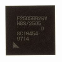
DF2505BR26DV Renesas Electronics America, DF2505BR26DV Datasheet - Page 458

DF2505BR26DV
Manufacturer Part Number
DF2505BR26DV
Description
IC H8S/2505 MCU FLASH 176-LFBGA
Manufacturer
Renesas Electronics America
Series
H8® H8S/2500r
Specifications of DF2505BR26DV
Core Processor
H8S/2000
Core Size
16-Bit
Speed
26MHz
Connectivity
I²C, SCI
Peripherals
POR, PWM, WDT
Number Of I /o
104
Program Memory Size
384KB (384K x 8)
Program Memory Type
FLASH
Ram Size
32K x 8
Voltage - Supply (vcc/vdd)
3 V ~ 5.5 V
Data Converters
A/D 16x10b; D/A 2x8b
Oscillator Type
Internal
Operating Temperature
-40°C ~ 85°C
Package / Case
176-LFBGA
Lead Free Status / RoHS Status
Lead free / RoHS Compliant
Eeprom Size
-
Available stocks
Company
Part Number
Manufacturer
Quantity
Price
Company:
Part Number:
DF2505BR26DV
Manufacturer:
Renesas Electronics America
Quantity:
10 000
- Current page: 458 of 980
- Download datasheet (6Mb)
Section 13 Serial Communication Interface (SCI)
13.3.7
SSR is a register containing status flags of the SCI and multiprocessor bits for transfer. 1 cannot
be written to flags TDRE, RDRF, ORER, PER, and FER; they can only be cleared. Some bit
functions of SSR differ between normal serial communication interface mode and Smart Card
interface mode.
• Normal Serial Communication Interface Mode (When SMIF in SCMR Is 0)
Rev. 6.00 Sep. 24, 2009 Page 410 of 928
REJ09B0099-0600
Bit
7
6
Bit Name
TDRE
RDRF
Serial Status Register (SSR)
Initial
Value
1
0
R/W
R/(W)*
R/(W)*
1
1
Description
Transmit Data Register Empty
Displays whether TDR contains transmit data.
[Setting conditions]
•
•
[Clearing conditions]
•
•
Receive Data Register Full
Indicates that the received data is stored in RDR.
[Setting condition]
•
[Clearing conditions]
•
•
The RDRF flag is not affected and retains their previous
values when the RE bit in SCR is cleared to 0.
If reception of the next data is completed while the RDRF
flag is still set to 1, an overrun error will occur and the
receive data will be lost.
When the TE bit in SCR is 0
When data is transferred from TDR to TSR and data
can be written to TDR
When 0 is written to TDRE after reading TDRE = 1*
When the DTC*
request and writes data to TDR
When serial reception ends normally and receive data
is transferred from RSR to RDR
When 0 is written to RDRF after reading RDRF = 1*
When the DTC*
transfers data from RDR
2
2
is activated by a TXI interrupt
is activated by an RXI interrupt and
3
3
Related parts for DF2505BR26DV
Image
Part Number
Description
Manufacturer
Datasheet
Request
R

Part Number:
Description:
KIT STARTER FOR M16C/29
Manufacturer:
Renesas Electronics America
Datasheet:

Part Number:
Description:
KIT STARTER FOR R8C/2D
Manufacturer:
Renesas Electronics America
Datasheet:

Part Number:
Description:
R0K33062P STARTER KIT
Manufacturer:
Renesas Electronics America
Datasheet:

Part Number:
Description:
KIT STARTER FOR R8C/23 E8A
Manufacturer:
Renesas Electronics America
Datasheet:

Part Number:
Description:
KIT STARTER FOR R8C/25
Manufacturer:
Renesas Electronics America
Datasheet:

Part Number:
Description:
KIT STARTER H8S2456 SHARPE DSPLY
Manufacturer:
Renesas Electronics America
Datasheet:

Part Number:
Description:
KIT STARTER FOR R8C38C
Manufacturer:
Renesas Electronics America
Datasheet:

Part Number:
Description:
KIT STARTER FOR R8C35C
Manufacturer:
Renesas Electronics America
Datasheet:

Part Number:
Description:
KIT STARTER FOR R8CL3AC+LCD APPS
Manufacturer:
Renesas Electronics America
Datasheet:

Part Number:
Description:
KIT STARTER FOR RX610
Manufacturer:
Renesas Electronics America
Datasheet:

Part Number:
Description:
KIT STARTER FOR R32C/118
Manufacturer:
Renesas Electronics America
Datasheet:

Part Number:
Description:
KIT DEV RSK-R8C/26-29
Manufacturer:
Renesas Electronics America
Datasheet:

Part Number:
Description:
KIT STARTER FOR SH7124
Manufacturer:
Renesas Electronics America
Datasheet:

Part Number:
Description:
KIT STARTER FOR H8SX/1622
Manufacturer:
Renesas Electronics America
Datasheet:

Part Number:
Description:
KIT DEV FOR SH7203
Manufacturer:
Renesas Electronics America
Datasheet:


