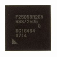
DF2505BR26DV Renesas Electronics America, DF2505BR26DV Datasheet - Page 224

DF2505BR26DV
Manufacturer Part Number
DF2505BR26DV
Description
IC H8S/2505 MCU FLASH 176-LFBGA
Manufacturer
Renesas Electronics America
Series
H8® H8S/2500r
Specifications of DF2505BR26DV
Core Processor
H8S/2000
Core Size
16-Bit
Speed
26MHz
Connectivity
I²C, SCI
Peripherals
POR, PWM, WDT
Number Of I /o
104
Program Memory Size
384KB (384K x 8)
Program Memory Type
FLASH
Ram Size
32K x 8
Voltage - Supply (vcc/vdd)
3 V ~ 5.5 V
Data Converters
A/D 16x10b; D/A 2x8b
Oscillator Type
Internal
Operating Temperature
-40°C ~ 85°C
Package / Case
176-LFBGA
Lead Free Status / RoHS Status
Lead free / RoHS Compliant
Eeprom Size
-
Available stocks
Company
Part Number
Manufacturer
Quantity
Price
Company:
Part Number:
DF2505BR26DV
Manufacturer:
Renesas Electronics America
Quantity:
10 000
- Current page: 224 of 980
- Download datasheet (6Mb)
Section 8 Data Transfer Controller (DTC)
8.4
Locate the register information in on-chip RAM (addresses: H'FFEBC0 to H'FFEFBF). Register
information should be located at an address that is a multiple of four within the range. Locating
the register information in address space is shown in figure 8.3. Locate the MRA, SAR, MRB,
DAR, CRA, and CRB registers, in that order, from the start address of the register information.
In the case of chain transfer, register information should be located in consecutive areas as shown
in figure 8.3, and the register information start address should be located at the vector address
corresponding to the interrupt source. Figure 8.4 shows the correspondence between the DTC
vector address and register information. The DTC reads the start address of the register
information from the vector address set for each activation source, and then reads the register
information from that start address.
When the DTC is activated by software, the vector address is obtained from: H'0400 +
(DTVECR[6:0] × 2). For example, if DTVECR is H'10, the vector address is H'0420.
The configuration of the vector address is the same in both normal* and advanced modes, a 2-byte
unit being used in both cases. These two bytes specify the lower bits of the register information
start address.
Note:
Rev. 6.00 Sep. 24, 2009 Page 176 of 928
REJ09B0099-0600
Normal mode is not supported in this LSI.
Register
information
start address
Chain
transfer
Location of Register Information and DTC Vector Table
Figure 8.3 Location of DTC Register Information in Address Space
MRA
MRA
MRB
MRB
0
CRA
CRA
Lower address
1
4 bytes
SAR
DAR
SAR
DAR
2
CRB
CRB
3
Register information
Register information
for 2nd transfer in
chain transfer
Related parts for DF2505BR26DV
Image
Part Number
Description
Manufacturer
Datasheet
Request
R

Part Number:
Description:
KIT STARTER FOR M16C/29
Manufacturer:
Renesas Electronics America
Datasheet:

Part Number:
Description:
KIT STARTER FOR R8C/2D
Manufacturer:
Renesas Electronics America
Datasheet:

Part Number:
Description:
R0K33062P STARTER KIT
Manufacturer:
Renesas Electronics America
Datasheet:

Part Number:
Description:
KIT STARTER FOR R8C/23 E8A
Manufacturer:
Renesas Electronics America
Datasheet:

Part Number:
Description:
KIT STARTER FOR R8C/25
Manufacturer:
Renesas Electronics America
Datasheet:

Part Number:
Description:
KIT STARTER H8S2456 SHARPE DSPLY
Manufacturer:
Renesas Electronics America
Datasheet:

Part Number:
Description:
KIT STARTER FOR R8C38C
Manufacturer:
Renesas Electronics America
Datasheet:

Part Number:
Description:
KIT STARTER FOR R8C35C
Manufacturer:
Renesas Electronics America
Datasheet:

Part Number:
Description:
KIT STARTER FOR R8CL3AC+LCD APPS
Manufacturer:
Renesas Electronics America
Datasheet:

Part Number:
Description:
KIT STARTER FOR RX610
Manufacturer:
Renesas Electronics America
Datasheet:

Part Number:
Description:
KIT STARTER FOR R32C/118
Manufacturer:
Renesas Electronics America
Datasheet:

Part Number:
Description:
KIT DEV RSK-R8C/26-29
Manufacturer:
Renesas Electronics America
Datasheet:

Part Number:
Description:
KIT STARTER FOR SH7124
Manufacturer:
Renesas Electronics America
Datasheet:

Part Number:
Description:
KIT STARTER FOR H8SX/1622
Manufacturer:
Renesas Electronics America
Datasheet:

Part Number:
Description:
KIT DEV FOR SH7203
Manufacturer:
Renesas Electronics America
Datasheet:


