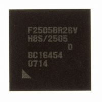
DF2505BR26DV Renesas Electronics America, DF2505BR26DV Datasheet - Page 732

DF2505BR26DV
Manufacturer Part Number
DF2505BR26DV
Description
IC H8S/2505 MCU FLASH 176-LFBGA
Manufacturer
Renesas Electronics America
Series
H8® H8S/2500r
Specifications of DF2505BR26DV
Core Processor
H8S/2000
Core Size
16-Bit
Speed
26MHz
Connectivity
I²C, SCI
Peripherals
POR, PWM, WDT
Number Of I /o
104
Program Memory Size
384KB (384K x 8)
Program Memory Type
FLASH
Ram Size
32K x 8
Voltage - Supply (vcc/vdd)
3 V ~ 5.5 V
Data Converters
A/D 16x10b; D/A 2x8b
Oscillator Type
Internal
Operating Temperature
-40°C ~ 85°C
Package / Case
176-LFBGA
Lead Free Status / RoHS Status
Lead free / RoHS Compliant
Eeprom Size
-
Available stocks
Company
Part Number
Manufacturer
Quantity
Price
Company:
Part Number:
DF2505BR26DV
Manufacturer:
Renesas Electronics America
Quantity:
10 000
- Current page: 732 of 980
- Download datasheet (6Mb)
Section 20 Flash Memory
System Control Register 2 (SYSCR2): SYSCR2 controls register accesses.
20.3.2
The programming/erasing interface parameter specifies the operating frequency, user branch
destination address, storage place for program data, programming destination address, and erase
block and exchanges the processing result for the downloaded on-chip program. This parameter
uses the general registers of the CPU (ER0 and ER1) or the on-chip RAM area. The initial value is
undefined at a power-on reset or in hardware standby mode.
When download, initialization, or on-chip program is executed, registers of the CPU except for
R0L are stored. The return value of the processing result is written in R0L. Since the stack area is
used for storing the registers except for R0L, the stack area must be saved at the processing start.
(A maximum size of a stack area to be used is 128 bytes.)
The programming/erasing interface parameter is used in the following four items.
1. Download control
2. Initialization before programming or erasing
Rev. 6.00 Sep. 24, 2009 Page 684 of 928
REJ09B0099-0600
Bit
7 to 4 ⎯
3
2
1, 0
Bit Name
FLSHE
⎯
⎯
Programming/Erasing Interface Parameter
Initial
Value
Undefined ⎯
0
Undefined ⎯
All 0
R/W
R/W
R/W
Description
Reserved
The write value should always be 0.
Flash memory control register enable
The access of the flash memory control register to the
CPU is controlled by writing 0. Setting 1 to FLSHE bit
enables reading/programming the flash memory control
register. When this bit is cleared to 0, the flash memory
control register is not selected. In this case, the content
of the flash memory control register is retained.
0: Flash control logic unit which controls H'FFFFA4 to
1: Flash control logic unit which controls H'FFFFA4 to
Reserved
The write value should always be 0.
Reserved
The write value should always be 0.
H'FFFFAF is disabled.
H'FFFFAF is enabled.
Related parts for DF2505BR26DV
Image
Part Number
Description
Manufacturer
Datasheet
Request
R

Part Number:
Description:
KIT STARTER FOR M16C/29
Manufacturer:
Renesas Electronics America
Datasheet:

Part Number:
Description:
KIT STARTER FOR R8C/2D
Manufacturer:
Renesas Electronics America
Datasheet:

Part Number:
Description:
R0K33062P STARTER KIT
Manufacturer:
Renesas Electronics America
Datasheet:

Part Number:
Description:
KIT STARTER FOR R8C/23 E8A
Manufacturer:
Renesas Electronics America
Datasheet:

Part Number:
Description:
KIT STARTER FOR R8C/25
Manufacturer:
Renesas Electronics America
Datasheet:

Part Number:
Description:
KIT STARTER H8S2456 SHARPE DSPLY
Manufacturer:
Renesas Electronics America
Datasheet:

Part Number:
Description:
KIT STARTER FOR R8C38C
Manufacturer:
Renesas Electronics America
Datasheet:

Part Number:
Description:
KIT STARTER FOR R8C35C
Manufacturer:
Renesas Electronics America
Datasheet:

Part Number:
Description:
KIT STARTER FOR R8CL3AC+LCD APPS
Manufacturer:
Renesas Electronics America
Datasheet:

Part Number:
Description:
KIT STARTER FOR RX610
Manufacturer:
Renesas Electronics America
Datasheet:

Part Number:
Description:
KIT STARTER FOR R32C/118
Manufacturer:
Renesas Electronics America
Datasheet:

Part Number:
Description:
KIT DEV RSK-R8C/26-29
Manufacturer:
Renesas Electronics America
Datasheet:

Part Number:
Description:
KIT STARTER FOR SH7124
Manufacturer:
Renesas Electronics America
Datasheet:

Part Number:
Description:
KIT STARTER FOR H8SX/1622
Manufacturer:
Renesas Electronics America
Datasheet:

Part Number:
Description:
KIT DEV FOR SH7203
Manufacturer:
Renesas Electronics America
Datasheet:


