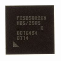
DF2505BR26DV Renesas Electronics America, DF2505BR26DV Datasheet - Page 836

DF2505BR26DV
Manufacturer Part Number
DF2505BR26DV
Description
IC H8S/2505 MCU FLASH 176-LFBGA
Manufacturer
Renesas Electronics America
Series
H8® H8S/2500r
Specifications of DF2505BR26DV
Core Processor
H8S/2000
Core Size
16-Bit
Speed
26MHz
Connectivity
I²C, SCI
Peripherals
POR, PWM, WDT
Number Of I /o
104
Program Memory Size
384KB (384K x 8)
Program Memory Type
FLASH
Ram Size
32K x 8
Voltage - Supply (vcc/vdd)
3 V ~ 5.5 V
Data Converters
A/D 16x10b; D/A 2x8b
Oscillator Type
Internal
Operating Temperature
-40°C ~ 85°C
Package / Case
176-LFBGA
Lead Free Status / RoHS Status
Lead free / RoHS Compliant
Eeprom Size
-
Available stocks
Company
Part Number
Manufacturer
Quantity
Price
Company:
Part Number:
DF2505BR26DV
Manufacturer:
Renesas Electronics America
Quantity:
10 000
- Current page: 836 of 980
- Download datasheet (6Mb)
Section 21 Clock Pulse Generator
21.9
21.9.1
As various characteristics related to the crystal resonator are closely linked to the user's board
design, thorough evaluation is necessary on the user's part, using the resonator connection
examples shown in this section as a guide. As the resonator circuit ratings will depend on the
floating capacitance of the resonator and the mounting circuit, the ratings should be determined in
consultation with the resonator manufacturer. The design must ensure that a voltage exceeding the
maximum rating is not applied to the oscillator pin.
21.9.2
When designing the board, place the crystal resonator and its load capacitors as close as possible
to the XTAL, EXTAL, OSC1, and OSC2 pins. Make wires as short as possible. Other signal lines
should be routed away from the oscillator circuit, as shown in figure 21.11. This is to prevent
induction from interfering with correct oscillation.
Figure 21.12 shows the recommended connection circuit between the power supply pins and Vss
pin. The CB which is a capacitor for stabilization should be inserted near the pin between the
power supply pins (V
P1V
Rev. 6.00 Sep. 24, 2009 Page 788 of 928
REJ09B0099-0600
CC
line. Other signal lines should not be crossed.
Usage Notes
Note on Crystal Resonator
Note on Board Design
Figure 21.11 Note on Board Design of Oscillator Circuit
CC
, V
CL
, P1V
Avoid
CC
, and P2V
C1
C2
Signal A Signal B
CC
) and Vss pin. Two CBs should be placed for the
EXTAL, OSC1
XTAL, OSC2
This LSI
Related parts for DF2505BR26DV
Image
Part Number
Description
Manufacturer
Datasheet
Request
R

Part Number:
Description:
KIT STARTER FOR M16C/29
Manufacturer:
Renesas Electronics America
Datasheet:

Part Number:
Description:
KIT STARTER FOR R8C/2D
Manufacturer:
Renesas Electronics America
Datasheet:

Part Number:
Description:
R0K33062P STARTER KIT
Manufacturer:
Renesas Electronics America
Datasheet:

Part Number:
Description:
KIT STARTER FOR R8C/23 E8A
Manufacturer:
Renesas Electronics America
Datasheet:

Part Number:
Description:
KIT STARTER FOR R8C/25
Manufacturer:
Renesas Electronics America
Datasheet:

Part Number:
Description:
KIT STARTER H8S2456 SHARPE DSPLY
Manufacturer:
Renesas Electronics America
Datasheet:

Part Number:
Description:
KIT STARTER FOR R8C38C
Manufacturer:
Renesas Electronics America
Datasheet:

Part Number:
Description:
KIT STARTER FOR R8C35C
Manufacturer:
Renesas Electronics America
Datasheet:

Part Number:
Description:
KIT STARTER FOR R8CL3AC+LCD APPS
Manufacturer:
Renesas Electronics America
Datasheet:

Part Number:
Description:
KIT STARTER FOR RX610
Manufacturer:
Renesas Electronics America
Datasheet:

Part Number:
Description:
KIT STARTER FOR R32C/118
Manufacturer:
Renesas Electronics America
Datasheet:

Part Number:
Description:
KIT DEV RSK-R8C/26-29
Manufacturer:
Renesas Electronics America
Datasheet:

Part Number:
Description:
KIT STARTER FOR SH7124
Manufacturer:
Renesas Electronics America
Datasheet:

Part Number:
Description:
KIT STARTER FOR H8SX/1622
Manufacturer:
Renesas Electronics America
Datasheet:

Part Number:
Description:
KIT DEV FOR SH7203
Manufacturer:
Renesas Electronics America
Datasheet:


