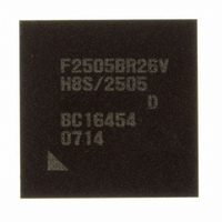
DF2505BR26DV Renesas Electronics America, DF2505BR26DV Datasheet - Page 537

DF2505BR26DV
Manufacturer Part Number
DF2505BR26DV
Description
IC H8S/2505 MCU FLASH 176-LFBGA
Manufacturer
Renesas Electronics America
Series
H8® H8S/2500r
Specifications of DF2505BR26DV
Core Processor
H8S/2000
Core Size
16-Bit
Speed
26MHz
Connectivity
I²C, SCI
Peripherals
POR, PWM, WDT
Number Of I /o
104
Program Memory Size
384KB (384K x 8)
Program Memory Type
FLASH
Ram Size
32K x 8
Voltage - Supply (vcc/vdd)
3 V ~ 5.5 V
Data Converters
A/D 16x10b; D/A 2x8b
Oscillator Type
Internal
Operating Temperature
-40°C ~ 85°C
Package / Case
176-LFBGA
Lead Free Status / RoHS Status
Lead free / RoHS Compliant
Eeprom Size
-
Available stocks
Company
Part Number
Manufacturer
Quantity
Price
Company:
Part Number:
DF2505BR26DV
Manufacturer:
Renesas Electronics America
Quantity:
10 000
- Current page: 537 of 980
- Download datasheet (6Mb)
Bit
4
3
2
Bit Name
NACKF
STOP
AL/OVE
Initial
Value
0
0
0
R/W
R/W
R/W
R/W
Stop Condition Detection Flag
Arbitration Lost Flag/Overrun Error Flag
Description
No Acknowledge Detection Flag
[Setting condition]
•
[Clearing condition]
•
[Setting conditions]
•
•
[Clearing condition]
•
This flag indicates that arbitration was lost in master mode
with the I
received while RDRF = 1 with the clocked synchronous
format.
When two or more master devices attempt to seize the bus
at nearly the same time, if the I
data differing from the data it sent, it sets AL to 1 to
indicate that the bus has been taken by another master.
[Setting conditions]
•
•
•
[Clearing condition]
•
When no acknowledge is detected from the receive
device in transmission while the ACKE bit in ICIER is 1
When 0 is written in NACKF after reading NACKF = 1
In master mode, when a stop condition is detected after
frame transfer
In slave mode, when a stop condition is detected after
the general call address or the first byte slave address,
next to detection of start condition, accords with the
address set in SAR
When 0 is written in STOP after reading STOP = 1
If the internal SDA and SDA pin disagree at the rise of
SCL in master transmit mode
When the SDA pin outputs high in master mode while a
start condition is detected
When the final bit is received with the clocked
synchronous format while RDRF = 1
When 0 is written in AL/OVE after reading AL/OVE=1
2
C bus format and that the final bit has been
Rev. 6.00 Sep. 24, 2009 Page 489 of 928
Section 14 I
2
C bus interface detects
2
C Bus Interface 2 (IIC2)
REJ09B0099-0600
Related parts for DF2505BR26DV
Image
Part Number
Description
Manufacturer
Datasheet
Request
R

Part Number:
Description:
KIT STARTER FOR M16C/29
Manufacturer:
Renesas Electronics America
Datasheet:

Part Number:
Description:
KIT STARTER FOR R8C/2D
Manufacturer:
Renesas Electronics America
Datasheet:

Part Number:
Description:
R0K33062P STARTER KIT
Manufacturer:
Renesas Electronics America
Datasheet:

Part Number:
Description:
KIT STARTER FOR R8C/23 E8A
Manufacturer:
Renesas Electronics America
Datasheet:

Part Number:
Description:
KIT STARTER FOR R8C/25
Manufacturer:
Renesas Electronics America
Datasheet:

Part Number:
Description:
KIT STARTER H8S2456 SHARPE DSPLY
Manufacturer:
Renesas Electronics America
Datasheet:

Part Number:
Description:
KIT STARTER FOR R8C38C
Manufacturer:
Renesas Electronics America
Datasheet:

Part Number:
Description:
KIT STARTER FOR R8C35C
Manufacturer:
Renesas Electronics America
Datasheet:

Part Number:
Description:
KIT STARTER FOR R8CL3AC+LCD APPS
Manufacturer:
Renesas Electronics America
Datasheet:

Part Number:
Description:
KIT STARTER FOR RX610
Manufacturer:
Renesas Electronics America
Datasheet:

Part Number:
Description:
KIT STARTER FOR R32C/118
Manufacturer:
Renesas Electronics America
Datasheet:

Part Number:
Description:
KIT DEV RSK-R8C/26-29
Manufacturer:
Renesas Electronics America
Datasheet:

Part Number:
Description:
KIT STARTER FOR SH7124
Manufacturer:
Renesas Electronics America
Datasheet:

Part Number:
Description:
KIT STARTER FOR H8SX/1622
Manufacturer:
Renesas Electronics America
Datasheet:

Part Number:
Description:
KIT DEV FOR SH7203
Manufacturer:
Renesas Electronics America
Datasheet:


