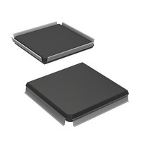
HD6417751RF240V Renesas Electronics America, HD6417751RF240V Datasheet - Page 1039

HD6417751RF240V
Manufacturer Part Number
HD6417751RF240V
Description
MPU 1.5/3.3V 0K PB-FREE 256-QFP
Manufacturer
Renesas Electronics America
Series
SuperH® SH7750r
Datasheet
1.D6417751RBP200DV.pdf
(1226 pages)
Specifications of HD6417751RF240V
Core Processor
SH-4
Core Size
32-Bit
Speed
240MHz
Connectivity
EBI/EMI, FIFO, SCI, SmartCard
Peripherals
DMA, POR, WDT
Number Of I /o
39
Program Memory Type
ROMless
Ram Size
48K x 8
Voltage - Supply (vcc/vdd)
1.4 V ~ 1.6 V
Oscillator Type
External
Operating Temperature
-20°C ~ 75°C
Package / Case
256-QFP Exposed Pad, 256-eQFP, 256-HQFP
Lead Free Status / RoHS Status
Lead free / RoHS Compliant
Eeprom Size
-
Program Memory Size
-
Data Converters
-
Available stocks
Company
Part Number
Manufacturer
Quantity
Price
Company:
Part Number:
HD6417751RF240V
Manufacturer:
Renesas Electronics America
Quantity:
10 000
- Current page: 1039 of 1226
- Download datasheet (7Mb)
22. PCI Controller (PCIC)
The PCICONF5 indicates the starting address of the memory space used by the PCI device. The
PCILAR0 specifies the starting address of the local address space 0. The PCILSR0 expresses the
size of the memory used by the PCI device. Regarding the method of setting each register, refer to
section 22.2, PCIC Register Descriptions.
For the PCICONF5 and PCILAR0, the most significant address bit that is higher than the memory
size set in the PCILSR0 becomes valid. The most significant address bit of the PCICONF5 and the
PCI address output from an external PCI device are compared for the purpose of determining
whether the access is made to the PCIC. When the addresses correspond, the access to the PCIC is
recognized, and a local address is generated from the most significant address bit of the PCILAR0
and the least significant bit of the PCI address output from the external PCI device. The PCI
command is executed for this local address.
If the most significant address bit of the PCI address output from the external PCI device does not
correspond with the most significant address bit of the PCICONF5, the PCIC does not respond to
the PCI command.
Address space 1 is, like address space 0, controlled by the PCICONF6, PCILSR1, and PCILAR1.
In this way, it is possible to set two address spaces. In systems with two or less local bus areas that
can be accessed from the PCI bus, separate address spaces can be allocated to each of them.
To make it possible to access two or more areas from the PCI bus, set the address spaces so that
multiple areas are covered. In this case, we can assume that the address space includes areas for
which no memory is installed. Note that, in this case, it is not possible to disable target transfers
to areas for which no memory is installed.
Note: See 22.3.11 (2), Target Read/Write Cycle Timing.
I/O-Read and I/O-Write Commands: The local registers of the PCIC are accessed by means of a
target transfer triggered by an I/O-read or I/O-write command. In the SH7751, accessing the local
registers by means of I/O transfer is made possible by setting a base address that specifies 1 Mbyte
of I/O space* in PCI configuration register 4 (PCICONF4). In the SH7751R, a base address that
specifies 256 bytes of I/O space should be set.
I/O-read and I/O-write commands only supports single transfers. The values of the byte-enable
signals (BE [3:0]) are ignored, and longword accesses are carried out inside the PCIC. When
executing an I/O-read and I/O-write commands transfer, specify B'0000 as the BE [3:0] value.
Note that some of the local registers are not accessible from the PCI bus. For details, see section
22.2, PCIC Register Descriptions.
Rev.4.00 Oct. 10, 2008 Page 939 of 1122
REJ09B0370-0400
Related parts for HD6417751RF240V
Image
Part Number
Description
Manufacturer
Datasheet
Request
R

Part Number:
Description:
KIT STARTER FOR M16C/29
Manufacturer:
Renesas Electronics America
Datasheet:

Part Number:
Description:
KIT STARTER FOR R8C/2D
Manufacturer:
Renesas Electronics America
Datasheet:

Part Number:
Description:
R0K33062P STARTER KIT
Manufacturer:
Renesas Electronics America
Datasheet:

Part Number:
Description:
KIT STARTER FOR R8C/23 E8A
Manufacturer:
Renesas Electronics America
Datasheet:

Part Number:
Description:
KIT STARTER FOR R8C/25
Manufacturer:
Renesas Electronics America
Datasheet:

Part Number:
Description:
KIT STARTER H8S2456 SHARPE DSPLY
Manufacturer:
Renesas Electronics America
Datasheet:

Part Number:
Description:
KIT STARTER FOR R8C38C
Manufacturer:
Renesas Electronics America
Datasheet:

Part Number:
Description:
KIT STARTER FOR R8C35C
Manufacturer:
Renesas Electronics America
Datasheet:

Part Number:
Description:
KIT STARTER FOR R8CL3AC+LCD APPS
Manufacturer:
Renesas Electronics America
Datasheet:

Part Number:
Description:
KIT STARTER FOR RX610
Manufacturer:
Renesas Electronics America
Datasheet:

Part Number:
Description:
KIT STARTER FOR R32C/118
Manufacturer:
Renesas Electronics America
Datasheet:

Part Number:
Description:
KIT DEV RSK-R8C/26-29
Manufacturer:
Renesas Electronics America
Datasheet:

Part Number:
Description:
KIT STARTER FOR SH7124
Manufacturer:
Renesas Electronics America
Datasheet:

Part Number:
Description:
KIT STARTER FOR H8SX/1622
Manufacturer:
Renesas Electronics America
Datasheet:

Part Number:
Description:
KIT DEV FOR SH7203
Manufacturer:
Renesas Electronics America
Datasheet:


