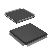
HD6417751RF240V Renesas Electronics America, HD6417751RF240V Datasheet - Page 634

HD6417751RF240V
Manufacturer Part Number
HD6417751RF240V
Description
MPU 1.5/3.3V 0K PB-FREE 256-QFP
Manufacturer
Renesas Electronics America
Series
SuperH® SH7750r
Datasheet
1.D6417751RBP200DV.pdf
(1226 pages)
Specifications of HD6417751RF240V
Core Processor
SH-4
Core Size
32-Bit
Speed
240MHz
Connectivity
EBI/EMI, FIFO, SCI, SmartCard
Peripherals
DMA, POR, WDT
Number Of I /o
39
Program Memory Type
ROMless
Ram Size
48K x 8
Voltage - Supply (vcc/vdd)
1.4 V ~ 1.6 V
Oscillator Type
External
Operating Temperature
-20°C ~ 75°C
Package / Case
256-QFP Exposed Pad, 256-eQFP, 256-HQFP
Lead Free Status / RoHS Status
Lead free / RoHS Compliant
Eeprom Size
-
Program Memory Size
-
Data Converters
-
Available stocks
Company
Part Number
Manufacturer
Quantity
Price
Company:
Part Number:
HD6417751RF240V
Manufacturer:
Renesas Electronics America
Quantity:
10 000
- Current page: 634 of 1226
- Download datasheet (7Mb)
14. Direct Memory Access Controller (DMAC)
(b) DDT Mode
Table 14.9 shows the memory interfaces that can be specified for the transfer source and transfer
destination in DMA transfer initiated by an external request supported by this LSI in DDT mode.
Table 14.9 External Request Transfer Sources and Destinations in DDT Mode
1
2
3
4
5
6
Notes: "SRAM-type" in the table indicates an SRAM, byte control SRAM, or burst ROM setting.
Bus Mode and Channel Priority Order
When, for example, channel 1 is transferring data in burst mode, and a transfer request is issued to
channel 0, which has a higher priority, the channel 0 transfer is started immediately.
If fixed mode has been set for the priority levels (CH0 > CH1), transfer on channel 1 is continued
after transfer on channel 0 is completely finished, whether cycle steal mode or burst mode is set
for channel 0.
If round robin mode has been set for the priority levels, transfer on channel 1 is restarted after one
transfer unit of data is transferred on channel 0, whether cycle steal mode or burst mode is set for
channel 0. Channel execution alternates in the order: channel 1 → channel 0 → channel 1 →
channel 0.
An example of round robin mode operation is shown in figure 14.11.
Rev.4.00 Oct. 10, 2008 Page 534 of 1122
REJ09B0370-0400
Synchronous DRAM
External device with DACK
Synchronous DRAM
SRAM-type, MPX, PCMCIA
SRAM-type, DRAM, PCMCIA,
MPX
SRAM-type, MPX, PCMCIA
Transfer Source
The only memory interface on which single address mode transfer is possible in DDT mode
is synchronous DRAM.
When performing dual address mode transfer, make the DACK output setting for the
SRAM, byte control SRAM, burst ROM, PCMCIA, or MPX interface.
*
DACK output setting in dual address mode transfer
Transfer Direction (Settable Memory Interface)
*
*
External device with DACK
Synchronous DRAM
SRAM-type, MPX, PCMCIA
Synchronous DRAM
SRAM-type, MPX, PCMCIA
SRAM-type, DRAM, PCMCIA,
MPX
Transfer Destination
*
*
Single
Single
Dual
Dual
Dual
Dual
Address
Mode
0, 1, 2, 3
0, 1, 2, 3
1, 2, 3
1, 2, 3
1, 2, 3
1, 2, 3
Usable
DMAC
Channels
Related parts for HD6417751RF240V
Image
Part Number
Description
Manufacturer
Datasheet
Request
R

Part Number:
Description:
KIT STARTER FOR M16C/29
Manufacturer:
Renesas Electronics America
Datasheet:

Part Number:
Description:
KIT STARTER FOR R8C/2D
Manufacturer:
Renesas Electronics America
Datasheet:

Part Number:
Description:
R0K33062P STARTER KIT
Manufacturer:
Renesas Electronics America
Datasheet:

Part Number:
Description:
KIT STARTER FOR R8C/23 E8A
Manufacturer:
Renesas Electronics America
Datasheet:

Part Number:
Description:
KIT STARTER FOR R8C/25
Manufacturer:
Renesas Electronics America
Datasheet:

Part Number:
Description:
KIT STARTER H8S2456 SHARPE DSPLY
Manufacturer:
Renesas Electronics America
Datasheet:

Part Number:
Description:
KIT STARTER FOR R8C38C
Manufacturer:
Renesas Electronics America
Datasheet:

Part Number:
Description:
KIT STARTER FOR R8C35C
Manufacturer:
Renesas Electronics America
Datasheet:

Part Number:
Description:
KIT STARTER FOR R8CL3AC+LCD APPS
Manufacturer:
Renesas Electronics America
Datasheet:

Part Number:
Description:
KIT STARTER FOR RX610
Manufacturer:
Renesas Electronics America
Datasheet:

Part Number:
Description:
KIT STARTER FOR R32C/118
Manufacturer:
Renesas Electronics America
Datasheet:

Part Number:
Description:
KIT DEV RSK-R8C/26-29
Manufacturer:
Renesas Electronics America
Datasheet:

Part Number:
Description:
KIT STARTER FOR SH7124
Manufacturer:
Renesas Electronics America
Datasheet:

Part Number:
Description:
KIT STARTER FOR H8SX/1622
Manufacturer:
Renesas Electronics America
Datasheet:

Part Number:
Description:
KIT DEV FOR SH7203
Manufacturer:
Renesas Electronics America
Datasheet:


