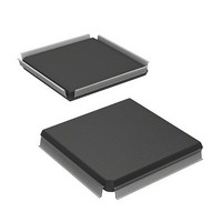
HD6417751RF240V Renesas Electronics America, HD6417751RF240V Datasheet - Page 371

HD6417751RF240V
Manufacturer Part Number
HD6417751RF240V
Description
MPU 1.5/3.3V 0K PB-FREE 256-QFP
Manufacturer
Renesas Electronics America
Series
SuperH® SH7750r
Datasheet
1.D6417751RBP200DV.pdf
(1226 pages)
Specifications of HD6417751RF240V
Core Processor
SH-4
Core Size
32-Bit
Speed
240MHz
Connectivity
EBI/EMI, FIFO, SCI, SmartCard
Peripherals
DMA, POR, WDT
Number Of I /o
39
Program Memory Type
ROMless
Ram Size
48K x 8
Voltage - Supply (vcc/vdd)
1.4 V ~ 1.6 V
Oscillator Type
External
Operating Temperature
-20°C ~ 75°C
Package / Case
256-QFP Exposed Pad, 256-eQFP, 256-HQFP
Lead Free Status / RoHS Status
Lead free / RoHS Compliant
Eeprom Size
-
Program Memory Size
-
Data Converters
-
Available stocks
Company
Part Number
Manufacturer
Quantity
Price
Company:
Part Number:
HD6417751RF240V
Manufacturer:
Renesas Electronics America
Quantity:
10 000
- Current page: 371 of 1226
- Download datasheet (7Mb)
10. Clock Oscillation Circuits
The function of each of the CPG blocks is described below.
PLL Circuit 1: PLL circuit 1 has a function for multiplying the clock frequency from the EXTAL
pin or crystal oscillation circuit by 6 (SH7751 and SH7751R) or 12 (SH7751R). Starting and
stopping is controlled by a frequency control register setting. Control is performed so that the
internal clock rising edge phase matches the input clock rising edge phase.
PLL Circuit 2: PLL circuit 2, according to the output clock feedback from the CKIO pin,
coordinates the phases of the bus clock and the CKIO pin output clock. Starting and stopping is
controlled by a frequency control register setting.
Crystal Oscillation Circuit: This is the oscillator circuit used when a crystal resonator is
connected to the XTAL and EXTAL pins. Use of the crystal oscillation circuit can be selected
with the MD8 pin.
Frequency Divider 1 (SH7751R only): Frequency divider 1 has a function for adjusting the clock
waveform duty to 50% by halving the input clock frequency when clock input from the EXTAL
pin is supplied internally without using PLL circuit 1.
Frequency Divider 2: Frequency divider 2 generates the CPU clock (Ick), bus clock (Bck), and
peripheral module clock (Pck). The division ratio is set in the frequency control register.
Clock Frequency Control Circuit: The clock frequency control circuit controls the clock
frequency by means of the MD pins and frequency control register.
Standby Control Circuit: The standby control circuit controls the state of the on-chip oscillation
circuits and other modules when the clock is switched and in sleep and standby modes.
Frequency Control Register (FRQCR): The frequency control register contains control bits for
clock output from the CKIO pin, PLL circuit 1 and 2 on/off control, and the CPU clock, bus clock,
and peripheral module clock frequency division ratios.
Standby Control Register (STBCR): The standby control register contains power save mode
control bits. For further information on the standby control register, see section 9, Power-Down
Modes.
Standby Control Register 2 (STBCR2): Standby control register 2 contains a power save mode
control bit. For further information on standby control register 2, see section 9, Power-Down
Modes.
Rev.4.00 Oct. 10, 2008 Page 271 of 1122
REJ09B0370-0400
Related parts for HD6417751RF240V
Image
Part Number
Description
Manufacturer
Datasheet
Request
R

Part Number:
Description:
KIT STARTER FOR M16C/29
Manufacturer:
Renesas Electronics America
Datasheet:

Part Number:
Description:
KIT STARTER FOR R8C/2D
Manufacturer:
Renesas Electronics America
Datasheet:

Part Number:
Description:
R0K33062P STARTER KIT
Manufacturer:
Renesas Electronics America
Datasheet:

Part Number:
Description:
KIT STARTER FOR R8C/23 E8A
Manufacturer:
Renesas Electronics America
Datasheet:

Part Number:
Description:
KIT STARTER FOR R8C/25
Manufacturer:
Renesas Electronics America
Datasheet:

Part Number:
Description:
KIT STARTER H8S2456 SHARPE DSPLY
Manufacturer:
Renesas Electronics America
Datasheet:

Part Number:
Description:
KIT STARTER FOR R8C38C
Manufacturer:
Renesas Electronics America
Datasheet:

Part Number:
Description:
KIT STARTER FOR R8C35C
Manufacturer:
Renesas Electronics America
Datasheet:

Part Number:
Description:
KIT STARTER FOR R8CL3AC+LCD APPS
Manufacturer:
Renesas Electronics America
Datasheet:

Part Number:
Description:
KIT STARTER FOR RX610
Manufacturer:
Renesas Electronics America
Datasheet:

Part Number:
Description:
KIT STARTER FOR R32C/118
Manufacturer:
Renesas Electronics America
Datasheet:

Part Number:
Description:
KIT DEV RSK-R8C/26-29
Manufacturer:
Renesas Electronics America
Datasheet:

Part Number:
Description:
KIT STARTER FOR SH7124
Manufacturer:
Renesas Electronics America
Datasheet:

Part Number:
Description:
KIT STARTER FOR H8SX/1622
Manufacturer:
Renesas Electronics America
Datasheet:

Part Number:
Description:
KIT DEV FOR SH7203
Manufacturer:
Renesas Electronics America
Datasheet:


